Nonvolatile memories based on AlO x embedded ZrHfO high- k gate dielectric
- PDF / 752,164 Bytes
- 6 Pages / 612 x 792 pts (letter) Page_size
- 42 Downloads / 403 Views
Nonvolatile memories based on AlOx embedded ZrHfO high-k gate dielectric Shumao Zhang1, Yue Kuo1, Xi Liu1,2, and Chi-Chou Lin1 1
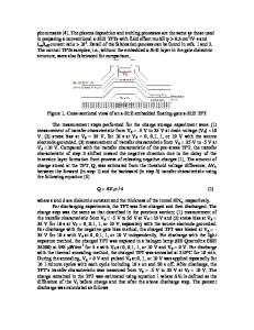
Thin Film Nano & Microelectronics Research Laboratory, Artie McFerrin Department of Chemical Engineering, Texas A&M University, College Station, TX 77843-3122, U.S.A. 2 Deptartment of Industrial and Systems Engineering, Ohio University, Athens, OH 45701, U.S.A. ABSTRACT MOS capacitors with the ZrHfO/AlOx/ZrHfO high-k gate dielectric stack were prepared and characterized for memory functions. The device prefers to trap holes, i.e., under the negative gate voltage, rather than electrons, i.e., under the positive voltage. The hole-trapping process is time and voltage dependent. The weakly trapped holes are quickly released upon the remove of the stress voltage. However, more than 30% of the originally trapped holes can be retained in the device after 10 years. The AlOx embedded ZrHfO high-k stack is a suitable gate dielectric structure for nonvolatile memories. INTRODUCTION The Si/oxide/nitride/oxide/Si (SONOS) gate dielectric structure has been widely studied as a possible replacement of the conventional floating-gate dielectric structure in the high density nonvolatile memory (NVM) ICs [1,2]. The programming speed and charge retention are major challenges for the SONOS-type memories [3,4]. In order to improve the charge-retention capability, Sugizaki et al. proposed to use Al2O3 to replace the silicon nitride (Si3N4) as the charge-storage layer to take advantage of the large energy barrier to prevent move the trapped electrons to the conduction band, i.e., 2.35 eV for the former and 1.39 eV for the latter [5]. Furthermore, Nakata et al. demonstrated that the nonstoichiometric Al-rich AlOx thin film is more effective in trapping charges than the stoichiometric Al2O3 film in the MONOS-structured device [6]. With the large band offsets between Si and SiO2, a high operating voltage is required to obtain the acceptable P/E efficiency, which causes a large leakage current [7]. When the SO2 control oxide in the NVM is replaced with a high dielectric constant (high-k) film, e.g., Al2O3 or HfO2, the programming and erasing voltages can be lowered [8,9]. In addition, the physically thicker HfO2 high-k can replace the sub 2 nm thickness SiO2 as the tunnel oxide layer, i.e., with the same equivalent oxide thickness (EOT), to reduce the current leakage problem [10]. Furthermore, it has been reported that the material and electrical properties of the metal oxide high-k gate dielectric can be improved by doping it with a third element to form the mixed oxide [11]. For example, the Zr-doped HfO2 (ZrHfO) film has a higher crystallization temperature, a lower interface density of states, and a larger effective k value than the undoped HfO2 film [11,12]. NVMs including the nanocrystals embedded ZrHfO control and tunnel oxides showed excellent memory functions [13-15]. In this paper, MOS capacitors containing the ZrHfO/AlOx /ZrHfO gate dielectric were fabricated and studied for memory functions. EXPERIMENT Th
Data Loading...