Adsorbate-induced enhancement of the spectral response in graphene/silicon-based Schottky barrier photodetectors
- PDF / 1,205,575 Bytes
- 6 Pages / 595.276 x 790.866 pts Page_size
- 53 Downloads / 294 Views
Adsorbate‑induced enhancement of the spectral response in graphene/silicon‑based Schottky barrier photodetectors N. Şahan1 · M. Fidan1 · C. Çelebi1 Received: 1 September 2020 / Accepted: 31 October 2020 © Springer-Verlag GmbH Germany, part of Springer Nature 2020
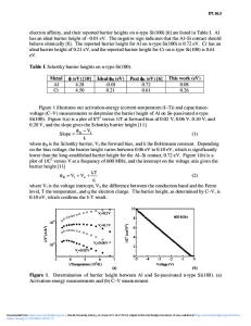
Abstract The impact of atmospheric adsorbates on the spectral response and response speed of p-type graphene/n-type Silicon (p-Gr/nSi) based Schottky barrier photodetectors are investigated. Wavelength resolved photocurrent and transient photocurrent spectroscopy measurements conducted under high-vacuum conditions revealed that the atmospheric adsorbates such as O 2 and H2O stuck on graphene electrode lead to hole doping in graphene and therefore shift its Fermi level towards higher energy states below its Dirac point. Such a shift in graphene’s Fermi level due to adsorbates increases the zero-bias Schottky barrier height of the p-Gr/n-Si heterojunction from 0.71 to 0.78 eV. Adsorbate induced increment in the barrier height promotes the separation of photo-generated charge carriers at the depletion region and leads to an improvement in the maximum spectral response (e.g., from 0.39 to 0.46 AW−1) and response speed of the p-Gr/n-Si photodetector in the near-infrared region. The experimentally obtained results are expected to give an insight into the adsorbate related variations in the rectification and photo-response characters of the heterojunctions of graphene and other 2D materials with different semiconductors. Keywords Graphene · Adsorbates · Schottky barrier · Spectral response
1 Introduction As a single-atom-thick two-dimensional material graphene has been considered to be employed as a transparent conductive electrode for semiconductor-based solar cells and broadband photodetectors due to its outstanding electrical conductivity and optical transmittance exceeding 97% in the spectral range between deep ultraviolet (UV) and far-infrared regions [1–5]. In addition to its intrinsic optical properties, the electronic transport and magnetic characteristics of single-layer graphene can be modified to a large extend by introducing adsorbates and defects in its hexagonally shaped crystal lattice [6–9]. It is known that a rectifying Schottky junction with a relatively large built-in potential of around 0.5–0.7 V is formed when single-layer graphene is coupled with most of the conventional semiconductors like Si, GaAs, and SiC [10–12]. A depletion layer accompanied by such a high built-in potential is created at the semiconductor side of the heterojunction. This indicates that graphene not only * C. Çelebi [email protected] 1
Quantum Device Laboratory, Department of Physics, İzmir Institute of Technology, Izmir 35430, Turkey
serves as a transparent electrode for charge carrier collection but also an active layer for electron–hole separation and hole transport. Electronic and optoelectronic characteristics of p-type graphene/n-type Si (p-Gr/n-Si) and p-type graphene/p-type Si (p-Gr/p-Si) heterojunctions with/without dielectric layer at the inter
Data Loading...