Electrical Characterization of the Oxide-Silicon Carbide Interface by MOS Conductance Technique
- PDF / 238,428 Bytes
- 5 Pages / 420.48 x 639 pts Page_size
- 0 Downloads / 330 Views
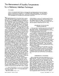
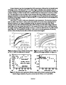
the conductance vs voltage (G-V) data for the metal-oxide-SiC (MOS) structure. It was found that the dry oxide contained too much charge either at the oxide-SiC interface or within the oxide films to obtain useful data. On the other hand the wet oxide invariably resulted in better capacitance and conductance data. The capacitance-voltage data showed that the SiC surface exhibited accumulation, depletion or inversion when the appropriate gate bias was applied. The conductance-voltage data indicate electronic surface states at the oxide-SiC interface. From this conductance data the interface state density has been estimated. INTRODUCTION The compound semiconductor 8-SiC has received considerable attention in recent years as a promising material for high-temperature and high-frequency electron devices. The recent successful growth of 6-SiC films on silicon substrate is a major step toward developing integrated circuits on SiC.
The study of oxide/SiC interface is very important for the development of MOS devices on SiC. One expects that the MOS on SiC will pose problems in common with other compound semiconductors, like GaAs, InP, etc. However,
there is a marked difference between the native oxides on SiC and other compound semiconductors: namely, the thermal oxide of SiC consists mostly of Si0 2. It is expected that the Si0 2 /SiC interface will be quite stable chemically. But it is the stability of the electrical properties of the interface that determines the success of MOS devices. The interface should have a minimum fixed oxide charge and surface state density. Very little work has been reported on the properties of the MOS made on SiC. Kee et al [1], have made MOS on a-SiC by thermal oxidation but were unable to induce a depletion layer even at large gate voltages. Suzuki et al [2] successfully fabricated MOS on 6H-SiC which showed accumulation,
depletion and inversion under the gate. In this paper we report the results of an investigation of oxide/SiC interface by MOS conductance technique [3].
EXPERIMENTAL The MOS structures were fabricated on a-SiC by growing both dry and wet thermal oxide at 1100°C for times between 60 and 150 minutes. The SiC samples were provided by NASA Lewis Research Center. These SiC films were grown on (100) silicon substrates by chemical vapor deposition [4]. The SiC films were 5 to 20 microns thick and the donor density was in the range of 1017 to 1018 cm- 3 . Prior to oxidation the samples were degreased and cleaned by the standard method. The wet oxide was grown by bubbling oxygen through a deionized water bath kept at the temperature between 90 and 95°C. The oxide film thicknesses ranged from 300 A to 1200 A. The oxide thickness was estimated from an Auger depth profile and by measuring MOS capacitance in the accumulation region.
Mat. Res. Soc. Symp. Proc. Vol. 54. 1•986Materials Research Society
562
Capacitance and conductance data were obtained by employing multifrequency LCR meters (models HP 4274A and 4275A) and a HP-9826 computer. Gate contacts were made using a mercur
Data Loading...