Electromigration in Epitaxial Copper Lines
- PDF / 350,242 Bytes
- 6 Pages / 612 x 792 pts (letter) Page_size
- 79 Downloads / 377 Views
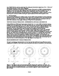
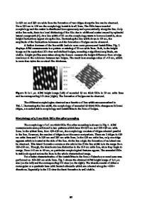
Electromigration in Epitaxial Copper Lines H.S. Goindi*, C.S. Shin§, M. Frederick*, Y. Shusterman†, H. Kim*, I. Petrov§, and G. Ramanath* * Department of Materials Science & Eng., Rensselaer Polytechnic Institute, Troy, NY 12180. † Department of Physics, Rensselaer Polytechnic Institute, Troy, NY 12180. § Materials Research Laboratory, University of Illinois, Urbana, IL 61801. ABSTRACT Copper is becoming the metal of choice for interconnect applications in integrated circuits due to its lower electrical resistivity and higher electromigration (EM) resistance. The effects of grain size, preferred orientation, and interfacial layers, on electromigration in Cu lines are, however, not yet well understood. In this paper, we compare the EM characteristics of epitaxial Cu(111) lines with that of polycrystalline lines with a (111) texture. We also investigate the effects of Ta, TaN and TiN interfacial underlayers and Cu crystal quality on the EM response of epitaxial Cu(001) lines. EM tests were carried out on 2-µm-wide Cu lines at a constant current density between 0.02 and 3.5 MA/cm2 in an Ar ambient at 300 °C. Our results indicate that EM resistance of both (111) and (001) epitaxial lines have a higher mean time to failure (MTTF) than polycrystalline Cu lines. The presence of a TiN or TaN interfacial layer increases the MTTF in Cu(001) films, while a Ta underlayer degrades EM resistance. X-ray diffractograms indicating a smaller full-width-at-half-maximum of Cu(001) films on nitride underlayers suggest that lower defect densities in these Cu films is the likely reason for improved EM resistance. Both (111) and (100) orientations fail by formation of faceted voids. INTRODUCTION Cu has replaced Al as the interconnect metal because of its higher electrical conductivity and greater resistance to electromigration (EM). EM is current-induced displacement of atoms caused by momentum transfer from mobile electrons to the atoms in the conductor[1], and has been extensively investigated in Al lines over the last three decades[2,3]. It is generally accepted that grain boundary diffusion is main mechanism for EM failure in Al lines, and large grains[4,5] having a (111) preferred orientation[6] and a bamboo-like morphology[7] show the highest resistance to EM. While the higher EM resistance of Cu can be explained by its higher melting point (lower grain boundary diffusivity),[8] the mechanism of EM-induced failures in Cu lines in not well understood. This is best illustrated by conflicting results reported by various groups. For instance, Ryu et al[9] have shown that Cu films with (111) preferred orientation show superior EM resistance while Vanasupa and co-workers [10] and Jo et al [11] have shown that the interfacial layer is the main variable and the preferred orientation is of no consequence. These studies are based on results obtained from polycrystalline films where the effects of grain size, orientation, and distribution are difficult to separate. Ideally, controlled experiments with epitaxial films of different orientations s
Data Loading...