Flame Annealing of Ion Implanted Silicon
- PDF / 2,425,629 Bytes
- 7 Pages / 417.6 x 639 pts Page_size
- 25 Downloads / 427 Views
FLAME ANNEALING OF ION IMPLANTED SILICON* J. NARAYAN AND R. T. YOUNG Solid State Division, Oak Ridge National Laboratory, Oak Ridge, TN 37830 ABSTRACT We have investigated flame annealing of ion implantation damage (consisting of amorphous layers and dislocation loops) in (100) and (111) silicon substrates. The temperature of a hydrogen flame was varied from 1050 to 1200°C and the interaction time from 5 to 10 seconds. Detailed TEM results showed that a "defect-free" annealing of amorphous layers by solid-phase-epitaxial growth could be achieved up to a certain concentration. However, dislocation loops in the region below the amorphous layer exhibited coarsening, i.e., the average loop size increased while the number density of loops decreased. Above a critical loop density, which was found to be a function of ion implantation variables and substrate temperature, formations of 900 dislocations (a cross-grid of dislocation in (100) and a triangular grid in (111) specimens) were observed. Electrical (Van der Pauw) measurements indicated nearly a complete electrical activation of dopants with mobility comparable to pulsed laser annealed specimens. The characteristics of p-n junction diodes showed a good diode perfection factor of 1.20-1.25 and low reverse bias currents. INTRODUCTION Annealing of ion implantation damage and electrical activation of dopants in semiconductors has been achieved with high-power lasers [1,2] and electron beams [3]. Two useful regimes of crystal growth for semiconductor processing have been clearly identified. First, the liquid-phase-epitaxial growth (LPE) that is involved during high-power pulsed laser irradiation, and second, the solidphase-epitaxial (SPE) growth involved in scanned continuous wave (CW) laser irradiation. The rates of crystal growth in the former case are of the order of several meters per second, while in the latter the maximum range is around a few tenths of a centimeter per second [4]. Recently, various other transient thermal sources such as high intensity arc lamps [5] and resistively heated graphite sources [6] have been employed to anneal displacement damage involving crystal growth in SPE regime. In this investigation, we have used a hydrogen flame to anneal displacement damage in arsenic and boron implanted silicon specimens. It was found that, below a certain dose of ion implantation, a complete annealing of displacement damage accompanied by a complete electrical activation of dopants was achieved. Above this dose, cross-grid or triangular network of edge dislocations was observed.
*Research sponsored by the Division of Materials Sciences, U. S. Department of Energy under contract W-7405-eng-26 with Union Carbide Corporation. Mat. Res. Soc. Symp. Proc.
Vol.
13 (1983)
Published by Elsevier
Science Publishing Co.,
Inc.
362
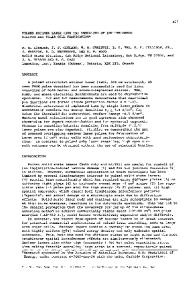
Fig. 1. Bright-field (B-F) electron micrograph showing a "complete" annealing if IhAs+ implanted of displacement damage (100 keV, 2.0 x 1•1 cm-), (001) silicon specimens, annealed by 1150%C flame (interaction time 10 s). Some dark patch
Data Loading...