Grain Structure and Electromigration Testing of Deep Sub- Micrometer Cu Interconnects
- PDF / 1,557,710 Bytes
- 6 Pages / 414.72 x 648 pts Page_size
- 87 Downloads / 519 Views
Mat. Res. Soc. Symp. Proc. Vol. 391 01995 Materials Research Society
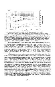
Grain structure test stripes were defined in linewidths of 140 nm, 240 rim, and 330 nm, all of 51 gm length. Substrates with test stripes were clamped onto a hot plate inside a vacuum chamber for annealing at a temperature of 375 'C and a pressure of 5x 10⁻⁷ Torr. Anneal times of 2.5 hours, 6 hours and 24 hours were performed. Grain structure was determined using a Hitachi S-4500 high-resolution field-emission scanning electron microscope (FESEM). Examination of micrographs of all linewidths and anneal times yielded grain size distribution for 54 randomly chosen grains per line. EM testing used constant voltage stressing in order to prevent arcing or runaway Joule heating, thus preserving any EM damage for post-mortem examination[13]. Groups of 25 parallel test stripes were prepared in linewidths of 230 nm and 380 nm having line lengths of 51 gm. These test stripes were stressed using the method described by Thompson and Cho for rapid EM evaluation[ 14]. The samples were stressed by a constant voltage and the total current through all 25 test stripes was measured. EM test stripes were stressed at a current density of 5x10 6 A/cm2 at a temperature of 275 'C in a vacuum of 5x 10'7 Torr. Total current was monitored for a duration of 100 hours. Post-mortem FESEM examination followed stress testing. RESULTS AND DISCUSSION Results of the as-deposited grain structure are shown in Fig. 1. The grain size distributions of the as-deposited Cu patterned in linewidths of 140 rnm, 240 nm and 330 nm are lognormal and there is no dependence of grain size distribution with linewidth. This is not surprising because even though the metal grains nucleate and grow within the confines of the photoresist stencil, the mean grain size of 38.5 nm is only a third of the linewidth of the smallest line and hence will not be affected by the stencil. The small mean grain size is due to the low substrate temperature during evaporation minimizing adatom surface mobility during deposition[15]. Upon long-term annealing, the grain size distributions changed to those shown in Fig. 2. During annealing, grains grew at the expense of neighboring grains eliminating some grains and reducing the dimensions of the smaller grains[ 16]. This occurred with a corresponding increase in 100-
TdCu Grain Structure As-Deposited
for Varyng Uneidths r
E5 E
Key
Grain Statistics:
w =330nm
a 0.
i•=38.5 nmn
xw14Ohm
A 101
1
10
22
I
40
703
Percent of Grains
Fig. 1. As-deposited grain size distribution for 140 rim, 240 nm, and 330 rn wide test stripes.
404
TI/Cu Grain Structure Alter 24 hour Anneal 0
._2
100-
.E
5
=nm 55
a
0.47
S••
w= 140 rr
.:_ 1
Cy= 0.60 w= 240 rm IA•= 52.8 nm cy= 0.45
Anneal Conditions: Temp. = 375 C Pressure = 5 x 10.7 Torr
Percent of Grains Fig. 2. Post-anneal grain size distributions for 140 nm, 240 nm, and 330 nm wide test stripes. the dimensions of the largest grains. This action resulted in an increase in median grain size, k., and an increase in
Data Loading...


