Heteroepitaxy of InSe/GaSe on Si(111) Substrates
- PDF / 1,379,396 Bytes
- 6 Pages / 612 x 792 pts (letter) Page_size
- 104 Downloads / 334 Views
GG4.5.1
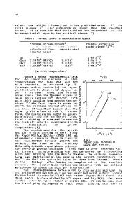
Heteroepitaxy of InSe/GaSe on Si(111) Substrates J. Jasinski, Z. Liliental-Weber, A. Chaiken1, G.A. Gibson1, K. Nauka1, C.C. Yang1, R. Bicknell2 Lawrence Berkeley National Laboratory, Materials Science Division, Berkeley, CA 94720, USA 1 Hewlett-Packard Laboratories, Palo Alto, CA, USA 2 Hewlett-Packard, Imaging and Printing Division, Corvallis, OR, USA ABSTRACT High quality growth of InSe on Si(111) was achieved by insertion of GaSe buffer layer. Rhombohedral polytypes were formed in both the InSe and GaSe layers. Twinning and stacking disorder was often detected in these materials due to their layered structure. Moreover, in samples with a thin GaSe layer, strong interdiffusion of indium into the GaSe layer was detected that resulted in the formation of an InxGaySe phase. The dominant threading defects present in these InSe/GaSe heterostructures were screw dislocations, which may act as nonradiative recombination centers. INTRODUCTION Due to its favorable structural and electrical properties, InSe is a candidate for application in a novel high density storage medium [1]. A silicon-process-compatible version of this device based on epitaxial InSe/GaSe/Si(111) heterojunction diodes has been constructed recently and a current gain of 65 has been demonstrated at an electron beam energy of 2 keV [2]. In this paper we investigate the structural properties of the InSe/GaSe heterostructures grown on Si(111) substrates. Both, InSe and GaSe are layered III-VI compounds consisting of stacks of identical sheets, each of which are composed of four atomic layers – two layers of group III (either Ga or In) sandwiched between two layers of Se. Each group III atom is bound through ionocovalent bonds with three, equally distant, neighboring Se atoms and with the equivalent group III atom from the next group III layer. There are no dangling bonds in this system although the sheets are bonded together only through weak van der Waals-like interactions. Different polytypes of these layered materials can be formed depending on the sheets’ stacking sequence. In the case of InSe and GaSe there are two commonly observed polytypes: (1) hexagonal ε-polytype (space group P63/mmc) with a stacking sequence described by ABAB; and (2) rhombohedral γ-polytype (space group R3m) with a stacking sequence described by Figure 1. Unit cells of hexagonal (a) ABCABC. Unit cells of these GaSe polytypes, and rhombohedral (b) polytype of projected along the [100] and [110] directions, are shown schematically in Fig. 1.
GG4.5.2
EXPERIMENTAL DETAILS Silicon wafers with exact (111) orientation as well as wafers with a 4 degree miscut were used as substrates for the InSe/GaSe growth. These wafers were cleaned prior to growth using a buffered-oxide etch or an ethanol/HF mixture. The GaSe growth was conducted at ~550oC. Temperature was then reduced to ~450oC and the InSe layer was grown on top of the GaSe film. Both films were grown from elemental Knudsen-cells. Several sets of samples with GaSe layer thicknesses ranging from 5-300 nm and InSe layer th
Data Loading...


