Initiation and Evolution of Epitaxial Growth of GaAs on CaF 2 /Si(111) Substrates
- PDF / 1,210,773 Bytes
- 6 Pages / 414.72 x 648 pts Page_size
- 0 Downloads / 393 Views
x 1.1
1.2
1.3
1.4
1.5
1.6
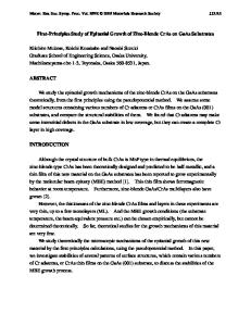
1000/T (1/K) Fig. I The growth modes of GaAs epitaxial layers, grown on on-axis CaF 2/Si(1 11) substrates. are plotted vs. As 2 flux and temperature. All samples were growvn at a rate of lILtm /hr. Three growth regimes are marked as A. B. and C. Epitaxial layers grown in regime C have the best quality. 59
Mat. Res. Soc. Symp. Proc. Vol. 317. @1994 Materials Research Society
regime, 2D nucleation was achieved. However, continued growth in the high temperature regime resulted in the formation of twins after epitaxial initiation. Between those two regimes, there is a temperature window in which high quality GaAs can be grown on the top of CaF 2/Si( 111). The size of this window is limited by 3D nucleation at lower temperature and twin defect formation at higher temperature. These two effects result in a narrow optimal growth window and complicate the growth. We previously reported observations that could be used to enlarge the optimal growth window.( 5 ) In this paper, we are going to address these issues with our new results and discuss their impact on the nucleation and evolution of GaAs epitaxial growth. II. GaAs Nucleation Under normal GaAs( 111 )B MBE growth conditions( 6 ), GaAs nucleates on the CaF 2( 111) surface in a 3D mode because GaAs(1 11) has larger surface free energy (-1400 ergs/cm 2) than CaF 2(111) (-500 ergs/cm2 ).(7 -8 ) In order to minimize the total free energy of the system, GaAs tends to form islands on the CaF 2( 11) surface. However, our research indicated that 2D nucleation of GaAs can be achieved on the CaF,/Si(Ill) surface when growing under high temperatures and high As 2 (or As 4 ) flux.( 4 -5 ) To understand this phenomenon, we designed an experiment which is illustrated schematically in the insert of Fig. 2. A CaF2 /Si(l 11) substrate was heated to a temperature Tmax, and remained at that temperature for 5 min with no incident As, beam. Then, the As 2 shutter was opened to allow the As 2 beam impinging on the sample for a period to. During this period the substrate temperature Ts was set at Tmax. After that, the sample was cooled down to room temperature. During the cooling process, the As 2 beam was shut off when Ts reached Tc (Tc - 400°C). Here, Tc is higher than the temperature at which the total reevaporation of physically adsorbed As species on the CaF2 ( 11) surface was observed. These samples then were taken out of the system and transferred to a separate analysis chamber which was coupled to a Dynamitron Accelerator, in order to do Rutherford backscattering spectrometry 0 T Tmax T2 ma v
I025
1Start
As, impinging Stop As2 impinging
-
I5
[
]
59
3 0O" T3 0-
to
3
As Impinging Time, to, (min) 2 4 6 8
C
F =4x 10"Smbar As
tt(min)o5
10
T=
0
2.0 0
2
>0.0
01.5
Data Loading...