Intrinsic and Dopant-Enhanced Solid Phase Epitaxy in Amorphous Germanium
- PDF / 542,800 Bytes
- 6 Pages / 612 x 792 pts (letter) Page_size
- 64 Downloads / 351 Views
1070-E05-06
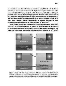
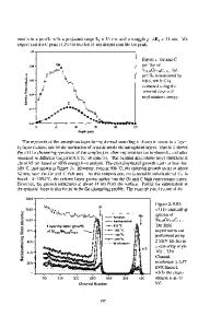
Intrinsic and Dopant-Enhanced Solid Phase Epitaxy in Amorphous Germanium Brett C. Johnson1, Paul Gortmaker2, and Jeffrey C. McCallum1 1 School of Physics, University of Melbourne, Swanston Street, Melbourne, Australia 2 Department of Electronic Materials Engineering, Australian National University, Canberra, Australia ABSTRACT The kinetics of intrinsic and dopant-enhanced solid phase epitaxy (SPE) are studied in thick amorphous germanium (a-Ge) layers formed by ion implantation on Ge substrates. The SPE rates for H-free Ge were measured with a time-resolved reflectivity (TRR) system in the temperature range 300 – 540 oC and found to have an activation energy of (2.15 ± 0.04) eV. Dopant enhanced SPE was measured in a-Ge layers containing a uniform concentration profile of implanted As spanning the concentration regime 1 - 10 x 1019 cm3. The generalized Fermi level shifting model shows excellent fits to the data. INTRODUCTION Crystallization of ion implanted materials via solid phase epitaxy (SPE) is a common processing step during device fabrication for its ability to achieve high dopant activation with a low thermal budget.[1] Ge is an ideal alternative to Si in which to gain unique insight into the SPE process.[2] Ge is also regaining importance due to recent developments in nano-scale electronics and opto-electrical devices.[3] However, unlike Si, only a few researchers have reported on SPE measurements in Ge.[2,4-9] SPE is a thermally activated process and the velocity of the crystalline-amorphous (c-a) interface through the amorphous phase can be described by an Arrhenius-type equation of the form, v = vo exp(-Ea/kT) where vo and Ea are the velocity pre-exponential factor and activation energy of SPE, respectively. The activation energies reported in previous studies range between 2.0 and 2.3 eV with a velocity prefactor lying between 6.1 x 10⁶ and 7 x10⁷ m/s. These factors are not yet known to an accuracy comparable to the corresponding Si values which are accepted to be 2.7 eV and 4.64 x 10⁷ m/s for H-free SPE.[10] Furthermore, the thickest a-Ge layers used to date in SPE measurements were 0.8 µm thick, while the majority of the measurements involved layers 0.5 µm or less in thickness. Roth et al. have demonstrated that hydrogen in-diffusion can effect the Si SPE rate for interface depths up to 2 µm.[10,11] Before the current study it was unclear whether the existing thin layer Ge SPE measurements were afflicted by the same problem. The very mechanism by which atoms rearrange during SPE is still an area of considerable debate. For Si at least, it has been shown that the SPE rate is sensitive to shifts in the Fermi level caused by the presence of dopants and that both neutral and charged defects may be responsible for the SPE process.[3,12-14] There have been very few studies on the SPE rates in dopant implanted a-Ge.[15] However, such information could be an important key to understanding the atomic rearrangement processes responsible for SPE. In this paper, we present comprehensive SPE measuremen
Data Loading...