Microstructural study of GaAs epitaxial layers on Ge(100) substrates
- PDF / 8,933,330 Bytes
- 10 Pages / 576 x 792 pts Page_size
- 73 Downloads / 354 Views
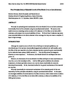
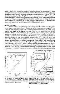
GaAs layers grown by close-spaced vapor transport on (100) Ge substrates have been investigated as a function of the experimental growth conditions. The effects on the micro structure of the surface preparation, substrate misorientation, and annealing were studied using optical microscopy and transmission electron microscopy. Microtwins and threading dislocations are suppressed by oxide desorption before deposition. Single domain GaAs layers have been obtained using a 50 nm thick double domain buffer layer on an annealed Ge substrate misoriented 3° toward [011]. The mismatch strain is mainly accommodated by dissociated 60° dislocations. These misfit dislocations extend along the interface by the glide of the threading dislocations inherited from the substrate, but strong interaction with antiphase boundaries (APB's) prevents them from reaching the interface. These results are discussed and compared with previous reports of GaAs growth on Ge(100).
I. INTRODUCTION Ge has attracted much attention in recent years as buffer layers to accommodate Si substrates with GaAs layers. Indeed, GaAs/Si composite structure combines the electronic and optical advantages of GaAs with the conventional and mature technology of silicon,1 but the epitaxial growth of GaAs on Si is not without inherent problems, including the antiphase disorder which occurs when a zincblende compound semiconductor is grown on an elemental diamond one, the 4.1 % lattice mismatch, and the 60% thermal expansion mismatch. Below the critical thickness, the lattice mismatch is entirely accommodated by elastic strain of the film. Beyond the critical thickness, the lattice mismatch is progressively accommodated by an array of misfit dislocations at the interface. The harmful influence of the misfit dislocations on device performance results from the formation of threading dislocations caused by the interaction of two or more nucleating misfit dislocations; the larger the lattice mismatch, the higher the probability of misfit dislocation interaction and subsequent formation of threading dislocation. The high threading dislocation density in GaAs-on-Si (106—108 cm"2), due to the 4.1% lattice mismatch, strongly affects minoritycarrier properties.2 Consequently, before GaAs-on-Si can be accepted as a viable technology in which high performance and reliable GaAs-based devices can be fabricated, the threading dislocation density has to be reduced. To reduce the threading dislocation density, there are techniques that attempt to improve an initially defective GaAs film (strained-layer superlattices3 or thermal treatments4-5) or those that attempt to modify the circumJ. Mater. Res., Vol. 10, No. 4, Apr 1995
http://journals.cambridge.org
Downloaded: 16 Mar 2015
stances of GaAs nucleation [two-step growth method6 or vicinal off-axis (100) surfaces7-8]. However, these techniques, combined or not, complicate considerably the device fabrication process and reduce the threading dislocation density at best by an order of magnitude. A more efficient approach to reduce drasti
Data Loading...