Pulsed Laser Annealing of Ion Implanted Ge
- PDF / 1,489,972 Bytes
- 6 Pages / 417.6 x 639 pts Page_size
- 90 Downloads / 424 Views
0. W. HOLLAND, J. NARAYAN, C. W. WHITE, B. R. APPLETON Solid State Division, Oak Ridge National Laboratory, Oak Ridge,
TN 37830
ABSTRACT Ion backscattering/channeling and transmission electron microscopy (TEM) were used to investigate the annealing behavior of ion implanted Ge single crystals using a Q-switched ruby The impurities studied were Bi, In, Sb and Pb, which were laser. implanted at liquid nitrogen temperature into both (100) and (111) crystal orientations. A rather unique damage structure which can form during room temperature implantation of Ge is discussed. Maximum substitutional concentrations, which far exceed the retrograde maxima, are reported for all the dopants The maximum concentrations were limited by studied in (100)Ge. an interfacial instability during epitaxial growth following laser irradiation which led to the formation of a well-defined cellular structure.
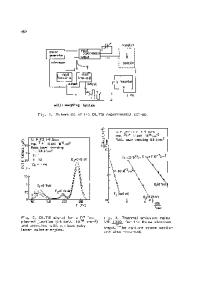
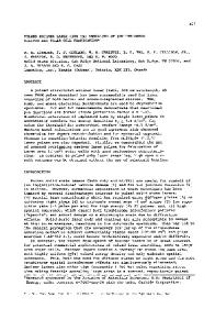
INTRODUCTION In a simple thermal Pulsed laser annealing has been actively studied in Si. melting model, the near surface region, < 1 pm thick, is envisioned to turn molten as a result of the deposited energy of the laser light. As this layer cools, epitaxial growth occurs on the crystalline substrate. Growth velocities between 1-6 m/sec, useful for device applications, have been achieved using Qswitched lasers. Crystalline material, free from extended defects, results from Phenomena such as dopant redistribution [2,3] and surthis rapid growth [1]. face segregation [4], solute trapping and metastable alloying [5,7], cell formation [5,7] and resolution of precipitated phases [81 have been observed after laser irradiation and have been cited as evidence in support of Our work extends the study of such phenomena to another the melting model. The annealing behavior of ion implanted, group(III,V) material germanium. dopants -In and Bi, as well as Sn and Pb are investigated using a pulsed ruby 2 laser with energy density = 1.3 J/cm and pulse duration = 15 nsec. One of the most important aspects of our study was the characterization of a unique damage structure which forms within the amorphous phase of Ge Figure 1 shows a sequence of cross-section, TEM during implantation [9]. micrographs from (111)Ge samples implanted with 120 key In ions at room temperature (RT) to progressively higher fluences. Part a) of the figure shows that a completely 2 amorphous overlayer has been formed by an implantation dose of 1 x 1015 cm- . An electron, micro-diffraction pattern from this overlayer in At a higher implant dose, Fig. lb shows that the layer is indeed amorphous. surface craters begin to form; craters as deep as 40 nm are evident in Fig Ic 2 5 (Fig. id), a very unique implant. At a dose of 5 x 10¹⁵ cmfor a 2 x 101 cmstructure has evolved which consists of regularly spaced pits or craters in the surface. The material surrounding these deep craters is amorphous as shown by diffraction techniques. Additionally, we found on exposure to ambient air that large amounts of carbon and oxygen are absorbed on the surface of the implanted *Research sponsored b
Data Loading...