Stress Reduction of Amorphous Silicon Deposited by PECVD
- PDF / 484,558 Bytes
- 8 Pages / 612 x 792 pts (letter) Page_size
- 38 Downloads / 498 Views
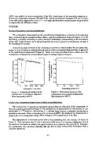
osition rate and stress with temperature variation in PECVD of α-Si. Regarding the variation of power, when this was increased from 15 to 25 W, the deposition rate also tended to increase, whilst with an increment in power from 25 to 30 W the deposition rate tended to decrease (Figure 2). An increment in power is associated with a better dissociation of silane gas; consequently, there are more reactive species in the plasma, increasing the deposition rate. The behavior of the stress followed similar trends. A likely explanation for this is that when the power is increased, the silicon atoms that form the film do not reach a good coverage, increasing the stress.
Figure 2. Deposition rate and stress with power variation in PECVD of α-Si. In the case of the pressure variation, with exception of 600-700 mTorr, an increase in the deposition rate is observed when pressure is raised (Figure 3). On the other hand, the stress decreases, reaching a minimum value at 900 mTorr and a maximum value at 700 mTorr. When
pressure is increased, the mean free path between atoms is reduced. Consequently, the atoms collide between them more frequently and more reactive species are presented during the process. Because of this, the deposition rate is improved.
Figure 3. Deposition rate and stress with pressure variation in PECVD of α-Si. Annealing treatment Figure 4 shows the mean residual stress change as a function of time of thermal annealing at 400 oC; all processes had the same behavior but for better visualization only processes 1, 3, 6, and 12 are shown. A high stress reduction is observed during the first two hours of annealing. By increasing the thermal annealing time even more, no considerable stress change is observed. In all cases, after 4 h of annealing the stress changes from compressive to tensile, and from that point onwards the latter type of stress continues to increase with time. Other researchers have reported [9] that the lowest stress is reached after 6 hours of annealing. Error bars are shown in one curve, where it is observed that the annealing treatment produces a uniform residual stress in the sample.
Figure 4. Stress reduction of α-Si as a function of thermal annealing time. With the results obtained, four deposition conditions were repeated, which corresponded to the lowest stress and the highest deposition rate. The deposition time was 60 minutes in order to obtain thicker films with lower stress. The gas flow was kept constant at 36 sccm for argon and at 100 sccm for silane; the temperature, power and pressure conditions employed are given in Table I. Table I. Best PECVD conditions for low stress and high deposition rate of α-Si. Process Temperature Power Pressure (°C) (Watts) (mTorr) 1
140
25
600
2
200
25
600
3
200
30
800
4
140
30
800
In this case, the thermal annealing times were 2, 2.5, 3 and 3.5 h at 400 oC. The obtained stress and its change with thermal annealing at different times are shown in Figure 5.
Figure 5. Stress reduction with time of thermal annealing in a second set of
Data Loading...