Synthesis of Single Crystal Bismuth-Telluride and Lead-Telluride Nanowires for New Thermoelectric Materials
- PDF / 1,385,174 Bytes
- 5 Pages / 417.6 x 639 pts Page_size
- 56 Downloads / 390 Views
Figure 1. Schematic of the nanowire growth apparatus.
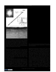
EXPERIMENTAL METHODS Synthesis of Nanowires Pulsed laser ablation (Spectra Physics GCR-16s, 355 nm or 532 nm) of targets composed of Bi 2Te 3 or PbTe was used to generate nanoclusters for 1D growth at thermodynamic nonequilibrium conditions. The growth apparatus is shown schematically in figure 1. The pressure in the growth chamber was kept at 100 - 250 torr. A mixture of Ar and H2 (10% H 2) was used as a buffer gas with a flow rate of about 100 sccm. The growth temperature is 530 'C for Bi 2Te 3, and 815 'C for PbTe. The products were collected on a substrate located behind the target. Structural Characterization of Nanowires The morphology and structure of the products were examined by field-emission scanning electron microscopy (SEM) (LEO 982), high-resolution transmission electron microscopy (TEM) and electron diffraction (Philips EM420). Energy dispersive X-ray (EDX) spectra were recorded with the TEM to evaluate the elemental compositions. Electrical Conductivity Measurement of Single Bi 2 Te3 Nanowires After registering the position of single Bi 2 Te 3 nanowires on oxidized Si substrates under SEM (JEOL JSM6400), electron beam resist was spun over the substrates and electron-beam lithography was used to define electrical leads to individual nanowires. After metalization of the leads I-V curves were obtained using Keithley 6517 electrometer and Keithley 220 programmable current source. RESULTS Bi 2Te 3 nanowires can be reproducibly prepared via vapor phase growth using our laser ablation method. Figure 2 shows SEM images of Bi 2Te 3 nanowires at different magnifications. They are faceted nanowires with diameters of 80 nm to 200 nm and lengths exceeding 10 ptm. TEM and electron diffraction studies (figure 3) show that the nanowires are single crystals. The diffraction pattern can be indexed to the hexagonal lattice of Bi 2Te3 (a = 4.385 A, c = 30.48 A) with the electron beam direction along [001] zone axis. A schematic illustration of Bi 2Te 3 structure viewed along the c axis superimposed on the TEM image of Bi 2Te 3 nanowire is shown in figure 3. These data show that the nanowires grow along the < 110> crystal direction. The single crystal nature and growth direction are further confirmed by high-resolution TEM measurements (figure 4). The lattice fringes in figure 4 are (101) crystal planes with an inter-
220
U
Figure 2. SEM images of Bi 2 Te 3 nanowires.
plane distance of 3.80 A. The angle between the fringes and the nanowire edge is 600, which is expected from the < 110> growth direction. EDX measurements show no other heavy elements except Bi and Te. Average atomic ratio of Te to Bi from 6 samples is 1.46. It gives a formula of Bi 2Te 2.92 . The deviation from Bi 2Te 3 is within our experimental error.
a
Figure 3. TEM image of a portion of Bi 2Te 3 nanowire with a schematic view of the Bi 2Te 3 structure in the ab plane superimposed on it. (inset) Electron diffraction pattern recorded along [001] zone axis.
Figure 4. High-resolution TEM micro
Data Loading...


