Tin Dioxide Films Prepared by a Rapid Chemical Vapor Deposition Method
- PDF / 240,291 Bytes
- 6 Pages / 414.72 x 648 pts Page_size
- 55 Downloads / 303 Views
225 Mat. Res. Soc. Symp. Proc. Vol. 363 01995 Materials Research Society
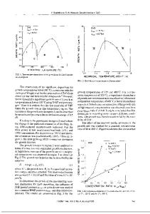
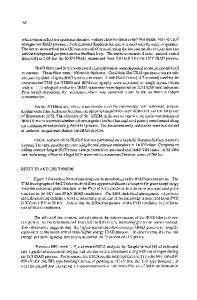
type heaters to avoid the condensation of the source material. Other experimental details are similar to those of our previous work 7 ' 8 III. Results and Discussion Figure 2 shows relationship between the vaporizing temperature of bis(2,4pentanedionato)tin and the deposition rate of SnO 2 films deposited at the substrate temperature (Ts) of 400'C. Deposition rate of SnO 2 films increased with increasing vaporizing temperature of the source material and reached at the maximum deposition rate of 440 nm min- 1 . This significant increase in the deposition rate results from the increase in vapor pressure of the source material with increasing vaporizing temperature, which leads to an increase in the number of SnO 2 nuclei deposited near or on the substrate. Thus, the deposition rate was confirmed to increase exponentially with increasing temperature. Figure 3 shows the relationship between the deposition rate of tin oxide and reciprocal temperature of the substrate. The deposition rate of SnO 2 films increased almost linearly from 60 to 180 nm min-. The apparent activation energy for the film formation was about 9.0 kJ molFigure 4 shows the X-ray diffraction patterns of tin dioxide films deposited at various substrate temperatures from Ts = 2000 to 600'C. These films obtained at the substrate temperature ranging from 3000 to 600'C had polycrystalline structures, while the film at Ts = 200'C was judged to be amorphous. The lattice constants of the films given by XRD from (101) and (211) planes were almost constant (Ts=300° to 600'C), and consistent with these from JCPDS card 12 (ao = 0.47382 nm, co = 0.31871 nm). Figure 5 shows the relationship between the substrate temperature and electrical resistivity of SnO 2 films. The resistivity of SnO 2 films decreased from 6.5X10- 2 Q•i at Ts = 250 0 C to 4.7X10⁻⁴Qm at Ts = 4000 C. In these polycrystalline films larger grain sizes are required to lower the resistivity of the films because of the decrease in the free carrier scattering at the grain boundaries. The transmission spectra of the film obtained at Ts = 2000 and 600'C in the wavelength range from 200 to 800 nm are shown in Figure 6. The transmittance of SnO 2 , deposited at Ts = 600'C, more than 70% in the wavelength range 400-800 nin. However, the transmittance of the film (400 nm thick) deposited at Ts = 200'C was low, and colored in yellow. Figure 7 shows the relationship between the refractive index ( X,=632.8 nm) of the films and substrate temperature. The refractive index was decreased with increasing substrate temperature. IV. Conclusion SnO 2 films were prepared rapidly by chemical vapor deposition under atmospheric pressure using bis(2,4-pentanedionato)tin. The important results of the present study are summarized as follows. 1.SnO 2 films obtained at Ts ranging from 300' to 600'C had polycrystalline rutile structure, while the film at T, = 200'C had amorphous one judging from the XRD pattern.
226
Table I. Experimental Conditions Fl
Data Loading...


