ZnO Based SAW Delay Line: Thin Film Characteristics and IDT Fabrication
- PDF / 894,074 Bytes
- 6 Pages / 612 x 792 pts (letter) Page_size
- 25 Downloads / 284 Views
D4.4.1
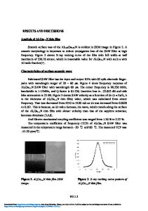
ZnO Based SAW Delay Line: Thin Film Characteristics and IDT Fabrication Farid Hassani1, Shahrokh Ahmadi1, Can E. Korman1, Mona Zaghloul1, Shiva Hullavarad2, R.D. Vispute2, T. Venkatesan2 1. Department of Electrical and Computer Engineering The George Washington University, Washington, DC 20052 2. Center for Superconductivity Research, Dept. of Physics, University of Maryland at College Park, College Park, MD 20742 Abstract: ZnO, a well-known piezoelectric material, is used to develop micro-scale Surface Acoustic Wave (SAW) delay line sensor. In this work, SAW delay line Devices are fabricated employing ZnO films that are deposited by RF sputtering technique. Films are characterized prior to device fabrication by X-Ray Diffraction (XRD) for film crystalline quality, UV-visible transmission spectroscopy for optical characteristics, and Atomic Force Microscopy (AFM) for surface morphology. Interdigital electrodes producing surface acoustic waves in the hundreds of MHz are developed by photolithography and metalization techniques. SAW delay line device testing, measurement and characteristics on RF sputtered ZnO films are presented and compared. Introduction SAW Sensors are based on piezoelectric materials and ZnO as a piezoelectric material has been widely used in SAW devices. ZnO film can be produced by different techniques such as Chemical Vapor Deposition (CVD), Pulsed Laser Deposition (PLD) and RF sputtering. Since high temperature steps can affect the performance of the sensor in which acoustic and electronic parts are made on a single chip, CVD is not suitable for these cases. In the case of sputtering, the sputtering variables such as chamber pressure, RF power, target-substrate distance and Ar/O2 ratio are very critical and they can affect the quality of film. In this work, we have investigated some properties of ZnO films as well as the effect of ZnO film quality on the IDT fabrication. Also the performance of SAW delay line have been measured and compared to theory. Theory As shown in Fig.1 SAW sensors basically consist of a piezoelectric material, two IDTs and a chemical interface. The input IDT generates while output IDT detects acoustic waves by employing the piezoelectric effect. The change of polymer characteristics due to gases exposure will cause a change in SAW phase velocity. Therefore, if a SAW sensor is placed in an oscillator loop, the phase velocity change will produce a shift in oscillation frequency.
Fig. 1 Basic SAW delay line
D4.4.2
The oscillation frequency can be obtained from the following equation [1]: fo= Vs/2p Where 2p is electrode periodicity, Vs is free surface velocity and also wavelength (λ) is equal to 2p. According to Smith’s Analysis of interdigital transducer [2], each IDT can be represented by a parallel circuit consisting of a radiation conductance Ga(f), an acoustic susceptance Ba(f) and transducer capacitance Ct. Fig. 2 shows this equivalent circuit. Ga(f), Ba(f) and Ct can be calculated from the following equations [3]: Ga(f) = Ga(fo) [Sin(x)/x]2 Ba(f) = Ga(fo)
Data Loading...