The use of ion implantation and annealing for the fabrication of strained silicon on thin SiGe virtual substrates
- PDF / 804,286 Bytes
- 11 Pages / 612 x 792 pts (letter) Page_size
- 41 Downloads / 367 Views
B1.6.1
The use of ion implantation and annealing for the fabrication of strained silicon on thin SiGe virtual substrates D. Buca, M.J. Mörschbächer, B. Holländer, M.Luysberg1, R. Loo2, M. Caymax2 and S. Mantl Institut für Schichten und Grenzflächen (ISG1) and cni - Center of Nanoelectronic Systems for Information Technology, Forschungszentrum Jülich (FZJ), D-52425 Jülich, Germany 1 Institut für Festkörperforschung (IFF), FZJ 2 IMEC, Kapeldreef 75, B-3001 Leuven, Belgium
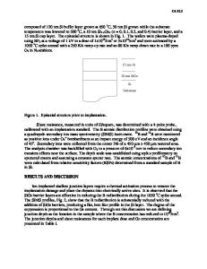
ABSTRACT Strain relaxed Si1-xGex layers are attractive virtual substrates for the epitaxial growth of strained Si. Tensile strained Si has attracted a lot of attention due its superior electronic properties. In this study, the strain relaxation of pseudomorphic Si1-xGex layers grown by chemical vapor deposition (CVD) on Si(100) substrates was investigated after He+ ion implantation and thermal annealing. The implantation induced defects underneath the SiGe/Si interface promote strain relaxation during annealing via preferred nucleation of dislocation loops which form misfit dislocations at the interface to the substrate. The amount of strain relaxation as well as the final threading dislocation density depend on the implantation dose and energy. Si1xGex layers with thicknesses between 75 and 420 nm and Ge concentrations between 19 and 29 at% were investigated. The strain relaxation strongly depends on the layer thickness. Typically the structures show ≈70 % strain relaxation and threading dislocation densities in the low 106 cm-2 range. AFM investigations proved excellent surface morphology with an rms roughness of 0.6 nm. The samples were investigated by Rutherford backscattering spectrometry, ion channeling, transmission electron microscopy and atomic force microscopy. INTRODUCTION Geometric downscaling of the device dimensions has led to an enormous increase in computing power. However, limitations due to excessive leakage, high power dissipation and exploding costs of the sophisticated chip fabrication tools became a major challenge. The implementation of more powerful new materials and device architectures is, therefore, considered as a promising alternative to improve CMOS performance. One of the most promising materials to boost the transistor performance is strained silicon. Its higher electron and hole mobilities [1] allow significantly higher drive currents of MOSFETs [2]. The most advanced method to realize strained silicon is the epitaxial growth of Si on a strain relaxed SiGe buffer layer. Due to the larger lattice constant of Si1-xGex the Si becomes tensely strained. The Si thickness, however, is limited by the critical thickness, when strain is relaxed by the generation of dislocations. The growth of relaxed SiGe layers with low defect density is a key problem. Most frequently, several µm thick compositionally graded Si1-xGex buffer layers are grown [3,4]. Such thick, compositionally graded buffer layers are nearly fully relaxed and exhibit threading dislocation densities of 104-107 cm-2. However, thick SiGe buffer layers are fairly
Data Loading...


