Thin Ni-Silicides for Low Resistance Contacts and Growth of Thin Crystalline Si Layers
- PDF / 572,178 Bytes
- 6 Pages / 612 x 792 pts (letter) Page_size
- 99 Downloads / 268 Views
Thin Ni-Silicides For Low Resistance Contacts And Growth Of Thin Crystalline Si Layers Elena A. Guliants and Wayne A. Anderson Department of Electrical Engineering, State University of New York at Buffalo, Buffalo, NY14260
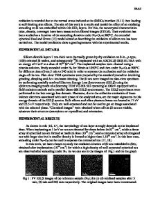
ABSTRACT A new technological method of producing the Ni silicide with metal-like conductivity by deposition of a thin Si film over an ultrathin Ni prelayer at low temperature has been developed. The interaction of a metallic Ni with the Si atoms provided by the deposition source leads to the formation of the Ni-rich silicide phases immediately after the onset of Si deposition. Continued Si deposition results in the transformation of the Ni-rich silicide phases into the more Si-rich ones which implies that the phase composition is controlled by the Ni-to-Si concentration ratio rather than temperature. After Ni is completely consumed, the Si grains grow epitaxially on the disilicide crystals. The silicide layer has been studied in detail with respect to both the dynamics of the silicide growth and the electrical properties. The Ni silicide resistivity was found to be 2x 10⁻⁴ Ω-cm. The technique has advantages in two respects: it provides a high crystallinity Si film and allows fabrication of an ohmic contact directly on the substrate thus leaving the front surface of the film available for the formation of the active device junction.
INTRODUCTION Metal silicides as ohmic contacts in Si-based technology introduced first in late 60s [1] continue to be a very topical subject for research [2,3]. NiSi2 is among the most extensively studied silicides because of its perfect thermal stability and a small lattice mismatch with Si (0.4%) which makes Ni disilicide the best suited for the epitaxial growth on a Si substrate [4]. Nowadays, much effort is focused on the self-aligned silicidation process (SALICIDATION) where NiSi2 is prepared by Ni deposition on a single crystal Si wafer followed by thermal annealing [5,6]. In such works, the NiXSiY phase formation and transformation was studied by varying the annealing temperature and, hence, was described in terms of thermodynamic processes as the well-known Ni2Si-NiSi-NiSi2 sequence [7]. The NiSi2 was shown to grow epitaxially on c-Si. This particular study is aimed at exploring the reverse process, namely silicon heteroepitaxy on NiSi2, where the formation of Ni disilicide takes place during Si deposition on a Ni film. Recently, several reports were made on the annealing of the Ni-implanted a-Si, and the enhanced Si crystallization was observed in the vicinity of the formed NiSi2 precipitates [8,9]. The metal-induced Si crystallization was observed also in the case of annealing of the a-Si covered with a thin Ni film [10,11]. Therefore, the technique introduced here may result in both enhanced Si crystal growth and self-organized and self-aligned NiSi2, which serves as a satisfactory back ohmic contact for various planar microelectronic devices such as, for example, diodes and solar cells. C7.14.1
Mat. Res. Soc. Symp. Vol. 611 © 2000 Materials Research Soci
Data Loading...