Wafer Level Chip Size Packaging Technology for Bulk Acoustic Wave Filters
- PDF / 796,707 Bytes
- 5 Pages / 612 x 792 pts (letter) Page_size
- 66 Downloads / 280 Views
0990-B07-14
Wafer Level Chip Size Packaging Technology for Bulk Acoustic Wave Filters Hajime Yamada, Naoko Aizawa, Hiroyuki Fujino, Yoshihiro Koshido, and Yukio Yoshino Murata Manufacturing Co., Ltd., 1-10-1 Higashikoutari, Nagaokakyo-shi, Kyoto, Japan
ABSTRACT Wafer level chip size packages (WL-CSP) have been successfully fabricated for bulk acoustic wave (BAW) filters. WL-CSP has been completed at the wafer level prior to dicing. Two silicon wafers are used as a die and a lid for chip size packaging. Both device and lid wafers have the same expansion coefficient and the package is strong enough to withstand the thermal stress. The package has a hermetic seal with copper-tin intermetallic bonding. The bonded wafers are then thinned by grinding. Via holes are formed by reactive ion etching (RIE) and filled by copper electroplating. The package has solder bumps on each terminal, ready for flipchip assembly. We have succeeded to produce CSP-BAW filters with a hermetically sealed cavity, which is 840 micrometers squared and 270 micrometers in height including solder bumps.
INTRODUCTION In electronic devices, an ever demanding trend toward smaller, lighter and thinner consumer products requires further package miniaturization compared to a conventional package [1]. The electronic packaging industry has evolved from surface-mount technology to a ball grid array (BGA) package for high throughput assembly of a wide variety of ICs, while at the same time allowing reduction of the pad pitch on the printed circuit board. The latest evolution in packaging refers to the wafer level chip size packaging techniques whose process is completed at the wafer level prior to dicing[1,2]. The advantage of the Wafer Level Chip Size Package (WL-CSP) is that they are fabricated and tested on the wafer, so the WL-CSP reduces the cost and size of devices compared with other packaging techniques that are assembled after separated into the individual die from the wafers. In this work, we have tried WL-CSP in order to miniaturize a Bulk Acoustic Wave (BAW) filter.
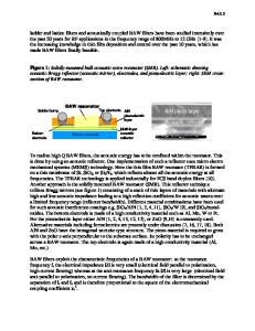
WAFER LEVEL CHIP SIZE PACKAGING TECHNOLOGY Figure 1 shows a schematic structure of a CSP BAW filter. Our chip size package consists of a lid, which contains a cavity over an active area of a BAW filter. Two silicon wafers are used as a die and a lid. Both device and lid wafers have the same expansion coefficient and the package is strong enough to withstand the thermal stress. The filter is hermetically packaged at the wafer level and sealed with copper-tin intermetallic bonding. The electrical connection goes through the wafer by via holes filled by copper electroplating. The interconnection between the via in the lid wafer and the pad on the device wafer is also carried out by copper-tin intermetallic bonding. The package has solder bumps on each terminal, ready for flip-chip assembly.
Solder bump for flip-chip assembly
Bonding for electrical interconnection Lid
Bonding for hermetic sealing
Cu filled via
BAW filter
Figure 1. Schematic structure of a CSP-BAW filter
Wafer b
Data Loading...


