A Survey of Defects in Strained Si Layers
- PDF / 1,504,585 Bytes
- 6 Pages / 612 x 792 pts (letter) Page_size
- 1 Downloads / 285 Views
B1.5.1
A Survey of Defects in Strained Si Layers S. W. Bedell1, H. Chen2, D. K. Sadana1, K. Fogel1 and A. Domenicucci2 IBM T.J. Watson Research Center, Yorktown Heights, NY 10598 2 IBM Microelectronics Division, Hopewell Junction, NY 12533 1
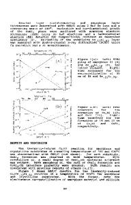
ABSTRACT A new method for highlighting defects in thin Si/SiGe layers is used to investigate the densities of various types of defects present in strained Si layers grown on relaxed SiGe layers. Defect densities were measured in strained Si layers formed on graded SiGe buffer layers (bulk), as well as silicon germanium-on-insulator substrates (SGOI), from both external and internal sources. The result of this investigation indicates that in addition to threading dislocations (TDs) and dislocation pile-ups, planar defects, i.e., stacking faults, are present in all but one of the materials studied. Due to the larger crystalline area affected by these planar defects, citation of only TD density as an indication of material quality is inadequate. A better measure of crystalline quality should include the density of TDs, pile-up clusters and planar defects (stacking faults) as well as some indication of the length distribution of the pile-ups and stacking faults. INTRODUCTION Recently, the use of strained silicon layers in high-performance CMOS circuits has been pursued as a possible pathway to improve transistor characteristics independently from device scaling [1-3]. The improved charge carrier transport properties in Si layers under tensile strain, compared to unstrained Si, are capable of providing a performance-enabling step for next generation bulk Si- or SOI-based CMOS technology. The adoption of this material into mainstream CMOS manufacturing will depend largely on the cost, availability and quality of strained Si substrates. Aside from process-related channel stressing techniques [4], the most common method of creating a strained Si layer is by using a relaxed SiGe alloy layer as a growth template. There have been several methods described in the literature for creating a relaxed SiGe layer on both bulk Si [5,6] as well as on a SiO2 layer to form SiGe-on-insulator (SGOI) [7-9]. The benefit of the latter is that the performance gain from both SOI and strained Si can be realized simultaneously. Common to most techniques for creating relaxed SiGe layers is their dependence on formation and growth of strain relieving defects which are ultimately responsible for strain relaxation. The methods described in the literature are differentiated by their techniques used to reduce the density of dislocations at the surface of the alloy. Typically, the figure of merit for relaxed SiGe quality is the density of threading dislocations (TDs) which intersect the alloy surface. Because threading defects cannot terminate within the crystal volume, subsequent epitaxial growth of Si (under tensile strain) would translate the TD through the Si layer. A single threading defect is generally assumed to be the threading arm portion of a perfect 60° dislocation. Simple glide of such dislocations res
Data Loading...