Deposition Of Uniform Size Metallic Nanoparticles For Use In Non Volatile Memories
- PDF / 5,671,819 Bytes
- 6 Pages / 612 x 792 pts (letter) Page_size
- 20 Downloads / 226 Views
0997-I03-08
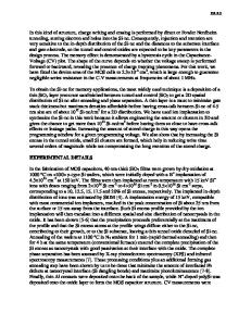
Deposition Of Uniform Size Metallic Nanoparticles For Use In Non Volatile Memories Emanuele Verrelli1, Dimitris Tsoukalas1, Konstantinos Giannakopoulos2, and Dimitris Ioannou3 1 Applied Physics and Mathematics, National Technical University of Athens, Heroon Polytechniou Str. 9, Zographou Campus, Athens, 15773, Greece 2 Material Sciences, NCSR Demokritos, Aghia Paraskevi, 15310, Greece 3 Electrical Engineering, George Mason University, Fairfax, VA, 22030 ABSTRACT In this work we investigate the non-volatile memory behavior of Ni nanoparticles embedded within an insulating matrix. Nickel nanoparticles are deposited at room temperature by a new high-vacuum technique over a 4 nm tunneling thermal SiO2 layer followed by the deposition of HfO2 as a control insulator. Memory windows of ~1.5V are observed in MOS capacitors at gate pulse voltages of 8V. Charge retention for write and erase state clearly indicate long time charge storage behavior. INTRODUCTION Nanoparticle memories have made their point during last years as a possible solution to overcome the scaling issue of non-volatile memories (NVM). Metallic nanoparticles have been less explored than semiconductor nanoparticles as charge storage elements [1, 2]. In principle metal nanoparticles should present advantages over silicon nanocrystal memories. The higher electron affinity of several metals as compared with Si allows for engineering the potential well of the storage nodes in order to create an asymmetric barrier between Si channel and the storage nodes. The usual method to form metallic nanoparticles is based on the deposition of thin metallic films using evaporation on top of a tunneling thermal oxide followed by thermal annealing resulting in the formation of metallic nanoparticles. The density and size distributions of the nanoparticles depend on annealing conditions and the thickness of the deposited thin film [3]. The drawback of this technique is the need for relatively high temperature treatment that involves the risk for contamination of the silicon substrate. It also results in uncontrolled size distribution of the nanoparticles. In this work we are presenting results on the formation of nickel nanoparticles on a thin tunneling thermal SiO2 layer using a new room temperature nanoparticle manufacturing technique. EXPERIMENT The nanoparticle deposition technique is based on a physical vacuum deposition (PVD) process. Particles are generated using a high-pressure magnetron sputtering device and carried away from the target area by the discharge gas into a condensation zone where nanoparticles are grown (Figure. 1). The nanoparticles after being swept through this zone enter the chamber through a final aperture and they are soft-landed on the oxide surface [4]. Using such a technique room temperature formation of nanoparticles becomes possible under high purity vacuum conditions. The tunneling oxide used in the present experiment is a thermal oxide of 4
nm formed after dry oxidation of p-type silicon wafers at 850˚C. Then a layer consisting
Data Loading...