Design and Performance Analysis of Core-Shell Dual Metal-Dual Gate Cylindrical GAA Silicon Nanotube-TFET
- PDF / 1,500,606 Bytes
- 9 Pages / 595.276 x 790.866 pts Page_size
- 94 Downloads / 348 Views
ORIGINAL PAPER
Design and Performance Analysis of Core-Shell Dual Metal-Dual Gate Cylindrical GAA Silicon Nanotube-TFET Umar Mushtaq 1 & Naveen Kumar 2
&
Sunny Anand 1 & Intekhab Amin 3
Received: 3 August 2019 / Accepted: 13 November 2019 # Springer Nature B.V. 2019
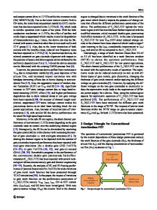
Abstract For experiencing phenomenon at nanoscale regimes, Nanotube FETs have been explored quite attentively due to their everincreasing application in low power electronics. Nanotubes have a unique property of forming a Gate All around configuration, which imparts the device with appropriate electrostatic control and at the same time providing it with a superior exemption from short channel effects. In this letter, we have proposed a Hetero Metal (HM)-Dual Gate (DG) All around Core-Shell (CS) Nanotube (NT) TFET. Different metal work functions for both the core and shell gates have been employed and compared the proposed device with a Single Metal Gate All around configuration. The HM-DG NT-TFET yielded better analog and RF characteristics like better ION (2.68X10⁻⁶A/μm), improved ION/IOFF (4.66X10¹²) and Subthreshold slope (19 mV/dec). The proposed device showed almost identical Cgg when compared to the Single Metal (SM) NT-TFET although transconductance (gm) and unity gain frequency (fT) were found to be far better than Single-Metal GAA Configuration that indicates towards the device being a propitious candidate in RF circuits. The devices were also compared based on linear parameters for which the proposed device exhibited superior results. Keywords Hetero metal . Dual-gate . Nanotube . Core-Shell . Linear parameters
1 Introduction TFETs, even after over a decade have been extensively investigated devices as they provide an outlet to combat the challenges faced due to intriguing scaling down of CMOS devices [1–3]. These challenges due to the aggressive scaling down of CMOS devices are faced in the form of difficulty in lowering the supply voltage (Drain Bias-VDS) and depreciation of the ION/IOFF ratio due to increased leakage currents. Due to a * Naveen Kumar [email protected] Umar Mushtaq [email protected] Sunny Anand [email protected] Intekhab Amin [email protected] 1
Amity University, Noida 201313, India
2
NIT Jalandhar, Punjab 144011, India
3
Jamia Millia Islamia, New Delhi, India
continuous reduction in transistor gate length, the supply voltage and the threshold voltage need to be minimized simultaneously for energy efficiency and better overdrive factor. TFETs have been keenly explored as being a reliable device enabling operations at very low voltages and minimizing the power dissipation loophole. TFET was also able to overcome the 60 mV/decade gridlock, which the MOSFET was incapable of achieving [2, 4, 5]. The gated p-i-n architecture of the TFET employs a quantum mechanical interband tunneling of charge carriers in contrast to the MOSFET where carrier transport is carried out by thermal injection by reducing or lowering the energy barrier. TFET carriers out the charge transport by interband tunneling wherein the device ca
Data Loading...