Mechanical Testing of Bonded Silicon on Insulator Wafers
- PDF / 1,463,061 Bytes
- 6 Pages / 420.48 x 639 pts Page_size
- 43 Downloads / 315 Views
MECHANICAL TESTING OF BONDED SILICON ON INSULATOR WAFERS. S.N. FarreM , B. Roberds*, M.C. Boettcher , M.S. Ismail , R.W. Bower , C.A. Desmond C.E. Hunt Mech. Aero. and Materials Engr. Dept., University of California, Davis, CA. Elect. and Comp. Engr. Dept., University of California, Davis, CA.
,
and
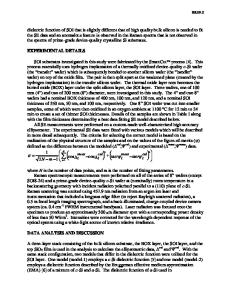
ABSTRACT A series of mechanical tests have been conducted on bonded silicon to silicon (native oxide present only) and oxide to oxide wafers at several times and temperatures. Tensile tests have been designed to evaluate the strength of the bond. Tensile tests have been conducted over the full range of bond strengths ranging from the weak van der Waals forces to the full silicon bonds. INTRODUCTION Recent develops in wafer bonding have opened the door for numerous three dimensional electrical, micromechanical devices, and high quality silicon on insulator materials. The first two applications are typically accomplished by fabricating one half of the device on the upper wafer and the remaining half of the device on the lower wafer. After chemical treatment an infrared aligner is used to align the partial circuits and bring them into contact. The wafers will immediately bond together with weak van der Waals type forces. The final step is an annealing step produces direct silicon bonding which processes the mechanical strength required for the given application. In the creation of silicon on insulator material an epitaxial layer is grown on one wafer and bonding to a handle wafer. After thermal annealing the device wafer is back thinned to the desired thickness. Of particular interest is the mechanical strength of the bonded materials as a function of the type of material, wafer preparation methods, and the time and temperature of the final anneal. The goal is to determine the minimum time and lowest temperature necessary to develop a desired bond strength. This goal both shortens the processing time and reduces or eliminates exposure to temperatures which may degrade other aspects of the device such as diffused or implanted layers. THEORETICAL DESCRIPTION The theoretical model of the bonding process suggests that the rate limiting steps in the bonding reaction is the formation of [SiOSi] bonds from the decomposition of silanol bonds.[l] The rate equation for this process is written as: d[SiOSi k(no - [SiOSi]) (I) dt where: k is the rate constant of the reaction, [SiOSi] is the concentration of SiOSi groups and no is the total number of bonding sites. Integration of this equation has the solution: [SiOSi ] (t) = n, [ I - exp(-kt') ] (2) where: x is taken as I for a reaction controlled process. If the ultimate tensile strength of the material is directly proportional to the number of [SiOSi] bonds then the following equation is derived for the fracture strength of the bond: o(t) = OmY.( 1 - exp(-ktx)) (3) where 0(t) is the fracture strength measured as a function of annealing time, ma is the maximum strength that the material will develop when the bonding is complete, and k sXthe rate constant. Because there is a base st
Data Loading...