Probing the metal gate high k interactions by backside XPS and C-AFM
- PDF / 3,128,714 Bytes
- 7 Pages / 612 x 792 pts (letter) Page_size
- 56 Downloads / 254 Views
Probing the metal gate high k interactions by backside XPS and C-AFM U.Celano1, T.Conard1, T.Hantschel1, W.Vandervorst1, 2 1
IMEC, Kapeldreef 75, B-3001 Leuven, Belgium. Instituut voor Kern- en Stralingsfysika, K.U. Leuven, Celestijnenlaan 200D, B-3001 Leuven, Belgium. 2
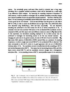
ABSTRACT The metal gate high k interaction is one of the dominant processes influencing the electrical performance (Vt, charge accumulation,..) of advanced gate stacks. These interactions are influenced by the entire thermal budget and the presence of reactive elements (on top/ within the material gate) such that relevant measurements can only be performed after a full processing cycle and on a complete gate stack. In such cases the relevant metal gate high k interface is a buried interface located below the metal gate (+ Si cap) and is not accessible for standard characterization methods like x-ray photoemission spectroscopy (XPS) due the limited escape depth of the photoelectrons. Moreover the presence of a conductive metal gate prevents the application of techniques such as conductive atomic force microscopy (C-AFM), to probe the local distribution of the defects, trapping sites and local degradation upon stressing. XPS in combination with layer removal steps like ion beam sputtering will destroy the bonding information and is thus not applicable. Chemical etching of the metal gate stack prior to the XPS measurements requires an extremely precious control of the etching in order to stop 1-2 nm before the high k metal interface. As an alternative we have developed a backside removal approach, that allows us to investigate using techniques such as XPS and C-AFM, the metal gate high k interface. INTRODUCTION With the downscaling of metal oxide semiconductor field effect transistor (MOSFET) devices, the usage of high k oxide has become mandatory, in order to achieve the required equivalent oxide thickness (EOT) as requested in the International Technology Roadmap for Semiconductor (ITRS) [1]. The properties of those new materials offer the possibility to achieve the right EOT but on the other hand represent several challenges compared to the traditional CMOS stack[2]. For instance as the high k oxide is replacing the SiO2-layer, a major concern impacting on device performance and properties, is the interaction of the metals used as gate material with the high k material leading to threshold voltage shifts, interface states, Fermi level pinning etc.. A detailed analysis of these materials interactions is therefore a prerequisite. In the present case the relevant interface is buried and located below the metal gate. For this reason the interfacial information and bonding structure is not accessible by standard characterization methods like XPS due to the limited escape depth of the photoelectrons or (timeof-fligth) secondary ions mass spectroscopy TOFSIMS or scanning probe microscopy SPM as these only probe the surface. Exposing deeper lying interfaces to these metrology tools then usually involves a dedicated sample preparation removing the top laye
Data Loading...