Advanced Al Damascene Process for Fine Trench Under 70nm Design Rule
- PDF / 474,158 Bytes
- 6 Pages / 595 x 842 pts (A4) Page_size
- 53 Downloads / 294 Views
B8.23.1
Advanced Al Damascene Process for Fine Trench under 70nm Design Rule Sung Ho Han, Kyung-in Choi, Sera Yun, Jeong Heon Park, Won Sok Lee, Sang Woo Lee, Gil Heyun Choi, Change Kee Hong, Sung Tae Kim, Uin Chung, Joo Tae Moon, and Byung-Il Ryu Process Development Team, Semiconductor R&D Center, Samsung Electronics Co. Ltd., San#24 Nongseo-Ri, Kiheung-Eup, Yongin-City, Kyungki-Do 449-711, Korea Phone: 82-31-209-3663, Fax: 82-31-209-6299, E-mail: [email protected]
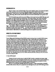
ABSTRACT Due to a rapid shrinkage in memory devices, backned of the line process experiences great difficulties, especially Al metallization. Furthermore, there is a continuous demands in low line resistance in order to promote device performances. In this article, Al damascene process is proposed as compared to Al patterning process, which suffers from inherent pattering issue at a fine pitch under 70nm. The most difficulties in the development of Al damascene process were to form a stable and void free Al in fine trench and to obtain scratch and corrosions free Al surface. In this study, 50nm beyond fill was successfully achieved by “bottom up growth” of CVD Al. For the process, CVD Al by using Methylpyrroridine Alane (MPA) precursor was deposited on a stacked film of CVD TiN and PVD TiN as a wetting layer, which was followed by PVD Al and reflow, then the Al surface was polished with colloidal silica based slurry. In addition, electrical property of Al scheme and W scheme was compared with damascene pattern, along with which we demonstrated that around 36% decrease in parasitic capacitance is achievable by decrease of metal line height from 3500A to 1000A on simulation test implying that device performance could be enhanced. INTRODUCTION Tungsten has been widely used for bit-line application but as design rule is scaled down, it could be problematic due to high resistance of metal wire. The high resistance mainly can be served by the height of metal line, which causes an increase in parasitic capacitance. From the results of a simulation test, by a decrease of metal wire height from 3500A to 1000A, we observed around 36% decrease in the parasitic capacitance, which is important in memory device requiring high-speed performance such as Nand-Flash, high speed SRAM etc. Accordingly, low resistance material; Al is a good candidate to reduce parasitic capacitance. However, an
B8.23.2
established process; Al Reactive Ion Etch (RIE) process has a difficulty in patterning process for fine metal line pattern in sub-70nm. For this reason, we believe that Al damascene process is a promising technology for fine metallization process. For sub-70nm, since conventional CVD Al process is not able to make void free Al fill in this design rule, we use a selective CVD Al deposition process depending on the condition of under layer.[1,2] In detail, CVD Al grows preferentially upward on the bottom in trench, so called, “bottom up growth” of CVD Al. The process sequence is that, at first, as a wetting layer, PVD TiN with a poor step coverage is stacked on CVD TiN
Data Loading...