Electromigration Reliability in Nanoscale Cu Interconnects
- PDF / 706,189 Bytes
- 11 Pages / 612 x 792 pts (letter) Page_size
- 64 Downloads / 654 Views
1036-M05-02
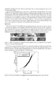
Electromigration Reliability in Nanoscale Cu Interconnects C.-K. Hu1, L. M. Gignac1, B. C. Baker-O'Neal1, G. Bonilla1, E. G. Liniger1, and P. L. Flaitz2 1 IBM T.J. Watson Research Center, Yortown Heights, NY, 10598 2 IBM Microelectronics Division, Hopewell Junction, NY, 12533 ABSTRACT Electromigration behavior in Cu damascene wires was studied for various Cu grain structures. The grain size was modulated by Cu linewidth and thickness, and by adjusting the wafer annealing process step after Cu electroplating and before Cu chemical mechanical polishing. A larger variation of Cu grain size between the samples was achieved on CMOS 65 nm node technology than previous nodes which was due to the finer line width and thinner metal thickness. The Cu lifetime and mass flow in samples with bamboo, near bamboo, bamboo-polycrystalline mixture, and polycrystalline grain structures were measured. The effects of a Cu(2.5 wt.% Ti) alloy seed, Cu surface pre-clean, and selective electroless CoWP deposition techniques on Cu electromigration were also observed and a significantly improved Cu lifetime was found. The electromigration activation energies for Cu in Cu(Ti) alloy, along Cu/amorphous a-SiCxNyHz interface and grain boundary were found to be 1.3, 0.95 and 0.79 + 0.05 eV, respectively. In addition the Cu line size effect on the Cu conductivity for Cu area less than 4x10⁴ nm2 was found to be a linear function of the Cu line area. INTRODUCTION Electromigration (EM) is a phenomenon of atom diffusion under electric potential gradient and EM in on-chip wirings has been extensively studied for several decades.[1-3] EM Cu mass flow is generated by diffusion under the influence of a dc current and can cause integrated circuit chip failure. The mass flow is determined by the effective Cu diffusivity and EM driving force. The effective Cu diffusivity in a Cu line is very sensitive to the Cu microstructure and is also dependent on fabrication conditions.[3] A typical Cu damascene interconnect has a top surface covered with a thin dielectric diffusion barrier layer and the bottom Cu surface and two sidewalls covered with a Ta-based liner.[4] Thus the fast diffusion paths in Cu damascene line along Cu/Ta interface, Cu/dielectric interface, and/or Cu grain boundaries have been reported.[3] However, the dominant diffusion path in Cu interconnections was found to be mostly along the Cu/dielectric cap interface for interconnects, but recent observations suggest that grain boundaries in addition to the Cu/dielectric interface diffusion could be diffusion paths for Cu lines with < 65 nm node technology.[5, 6] It is customary to label a technology node as ~0.7 of the minimal metal line width dimension; for example, the 45 nm CMOS technology node has a minimum metal line width of 70 nm. It is the near bamboo- or bamboo-like Cu grain structure observed in lines with 65 nm node technologies and greater that does not always exist for < 65 nm node interconnects. [6-9] Polycrystalline grain structure section coupling with bamboograin structu
Data Loading...