In Situ Cross-Sectional Scanning Tunneling Microscopy Sample Preparation Technique
- PDF / 2,915,622 Bytes
- 6 Pages / 414.72 x 648 pts Page_size
- 104 Downloads / 432 Views
Mat. Res. Soc. Symp. Proc. Vol. 399 ©01996 Materials Research Society
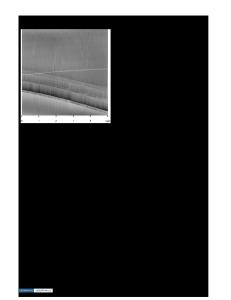
movement along the Z-axis. The piezoelectric sensitivities for the X/Y- and Z-directions are 19 nm V- 1 and 11 nm V- 1 respectively. Examination of the cross-sectional area of an 1001) wafer sample requires that the sample be repositioned in a modified sample holder, that consists of a stainless steel block and washer as exhibited in the inset in Fig. 1. For 100 micron thick 1001 )-oriented semiconductor wafer samples, prepared as described above, this positions the sample so that a I 110}-type plane is piezoelectric tube scanner
sample holder stage
A,
•stainless steel block stainless steel washer
010
Z
bent STM tip [0011
sample holder
sample orientation
x
Figure 1.Perspective view of the STM sample stage with modified sample and tip holders: note the 900 bent STM tip. The inset shows the sample orientation for cross-sectional scanning. oriented on the X-Y plane. To eliminate residual stresses and scratches, the XSTM samples are heated at a rate of 1VC min- 1 to 150 0C, and then held at this temperature for five hours. The STM tip required modification to perform scratching on an {001 )-type face of a sample. These modifications are outlined in Fig. 1.The scratch was produced using either a tungsten or a conducting diamond tip. The tungsten tip was fabricated from a 0.5 mm diameter tungsten wire that was electrochemically etched to a sharp point, and the diamond tip, produced from a mechanically ground boron-doped conducting diamond chip, was purchased from Digital Instruments (Santa Barbara, CA). These tips were bent at 90' angles and spot welded to standard OMICRON tip holders. In this configuration, the conducting tips can also be used to perform scanning on an {001) face to examine the scratch characteristics. Scanning an 1001 )-type surface in this configuration requires that the wiring of the STM scanner piezoelectric and feedback system be changed from their standard configurations. In this case, the Y- and Z-direction motions execute rastering, while the X-direction motion controls the sample-to-tip distance. To operate in this configuration, the functions of the X and Z finepiezoelectric controls are interchanged; the X voltage is changed to control the sample-tip separation and the Z voltage, which expands and contracts the scanner tube, is changed to couple with the Y voltage to perform rastering across the sample plane. To successfully induce cleavage, the sample is brought towards the 90' bent tip until contact is made. With the feedback loop off, further approach forces an indentation in the surface due to the tip. Varying the offset voltage in the modified X-direction drives the tip into the surface in a highly-controlled manner. The level of applied force can be increased for relatively hard samples or for increased indentation depth. After an indentation is created, the tip is drawn along the Y-direction (parallel to [ 1O]) either manually by applying an offset voltage to the Y-direction or automatically by setting th
Data Loading...