Thermal Oxidation of Cu Interconnects Capped with CoWP
- PDF / 1,401,038 Bytes
- 6 Pages / 612 x 792 pts (letter) Page_size
- 48 Downloads / 563 Views
B6.11.1
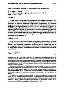
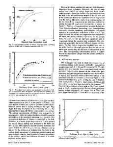
Thermal oxidation of Cu interconnects capped with CoWP J. Gambino, S. Smith**, S. Mongeon, D. Meatyard, F. Chen, P. DeHaven* IBM Microelectronics, 1000 River Street, Essex Junction, VT, 05452 ** IBM Thomas J. Watson Research Center, Yorktown Heights, NY 10598 *IBM Microelectronics, 1580 Route 52, Hopewell Junction, NY 12533 ABSTRACT The thermal oxidation of Cu interconnects, at 350oC in air, has been studied as a function of thickness of a CoWP capping layer. For thin CoWP layers (25 nm), a thick oxide layer (200 nm) is formed which is mainly composed of Cu2O. For thick CoWP layers (50 nm), the oxide layer is much thinner (36 nm) and is mainly composed of CoO. For both CoWP thicknesses, depletion of the underlying Cu is often observed after oxidation and whisker growth is often observed on the surface. The results are consistent with an oxidation mechanism where metal is the dominant diffusing species. For thin CoWP layers, Cu diffuses more quickly to the surface than Co, and therefore mainly Cu oxides are formed. For thick CoWP layers, the Cu diffusion to the surface is greatly reduced, and as a result, mainly Co oxides are formed. These results indicate that CoWP is not a good barrier for thermal oxidation, so high temperature exposure to oxidizing ambients must be minimized during processing of integrated circuits where CoWP is used instead of a dielectric barrier. INTRODUCTION Copper interconnects have gained wide acceptance in the microelectronics industry due to improved resistivity and reliability compared to Al interconnects [1]. However, as devices shrink, the wiring capacitance becomes an increasingly large percentage of the overall capacitance, resulting in increased delay, power consumption,and noise [2]. Therefore, low-k dielectrics will be widely used at the 90 nm technology node and beyond. Unfortunately, the effective dielectric constant is higher than that of the low-k dielectric, due to the SiN or SiCbased capping layers that are required to passivate the Cu surface [3]. Recently it has been shown that the circuit delay can be reduced by using a self-aligned CoWP cap instead of a dielectric cap [4]. The CoWP is formed selectively on Cu using electroless plating [5,6]. However, it is still unclear whether a CoWP cap by itself (with no dielectric cap) can provide an adequate barrier during oxidizing processes such as dielectric deposition and resist strip. During the deposition of oxide-based dielectrics by plasma enhanced chemical vapor deposition (PECVD), the CoWP will be briefly exposed to an oxidizing ambient at temperatures of 350 to 400oC. Both Cu [7,8] and Co [9,10] are known to oxidize at low temperatures (< 400oC). Oxidation of the Cu or the CoWP could lead to lower yield or reduced stress migration of electromigration lifetimes. Therefore, it is important to understand the oxidation behavior of Cu interconnects that are capped by CoWP. In this study, CoWP capped Cu interconnects are exposed to a 350oC oxidation, and the resulting microstructure is characterized. It is shown that ei
Data Loading...