Silicon Single-Electron Transistors and Single-Electron CCD
- PDF / 761,509 Bytes
- 11 Pages / 612 x 792 pts (letter) Page_size
- 35 Downloads / 307 Views
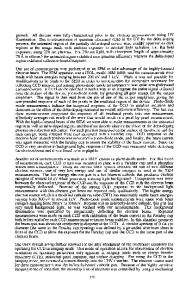
the input and the power supply voltage. Although the switching speed is low in this measurement, it is not limited by the inverter itself, but just by the slow response of the external circuit due to the large capacitance in the measurement system. Multiple-valued operation by combining SET with MOSFET The oscillatory conductance characteristics as a function of gate voltage may be applicable to multiple-valued logic or memory. In order to obtain multiple stability points by using multipeak characteristics, they should be multipeak negative differential resistance (NDR), not gate-voltage-induced resistance oscillation. We developed a new method to achieve SETbased NDR device consisting of a SET and a MOSFET [19]. The equivalent circuit of the device is shown in Fig. 8. The source of a MOSFET is
Figure 8. SET.
A schematic of multiple-valued memory circuit composed of a MOSFET and a
Figure 9. Measured Id-Vg characteristics of a SET and a MOSFET used for multiple-valued memory operation. A7.1.7
Figure 12. Demonstration of single-hole manipulation. (0, 1) and (1, 0) correspond to states in which a single hole exists under the right-hand front gate (MOSFET 1) and under the left-hand fine gate (MOSFET 2), respectively. gate voltage was applied to sense the current. Next, the upper-gate voltage was removed to eliminate electrons from wire regions, and then negative voltage was applied to the gate of MOSFET 1. This caused the transfer of the hole from MOSFET 2 to MOSFET 1, which was confirmed from the fact that current 2 became low but current 1 became high. In Fig. 12, we repeated the transfer and sensing of the hole. It is confirmed that an elementary-charge detection is actually possible with just a small wire MOSFET. In addition, this is the first demonstration of elementary-charge manipulation in a small Si CCD [4]. CONCLUSION We have developed a unique method for fabricating Si SETs named PADOX. The method utilize a special oxidation phenomenon that occurs when a very small Si structure is thermally oxidized. It is advantageous that tunnel barriers are formed automatically in a self-aligned manner. By using the methods, several kinds of single-electron-device operations were demonstrated, where we exploited the special features of SET, such as periodic current oscillation as a function of gate voltage. We have also proposed a new method for detecting and manipulating an elemental charge without tunnel barriers. We demonstrated that a single hole can be detected by utilizing the electron-hole system in a small Si-wire MOSFET and that an elementary charge can be transferred like in a CCD. This may allows us to establish a single-electron logic like a singleelectron binary-decision-diagram logic, where an elementary charge would act as a one-bit messenger. The devices demonstrated here will create high functionality with low power consumption for future LSIs.
A7.1.10
ACKNOWLEDGMENT The authors thank Dr. Katsutoshi Izumi, Dr. Takahiro Makino and Dr. Katumi Murase for their continued encouragement and Dr. Michiha
Data Loading...