Analysis of Leakage Currents through PLD Grown Ultrathin a-LaGdO 3 Based High-k Metal Gate Devices
- PDF / 962,580 Bytes
- 7 Pages / 612 x 792 pts (letter) Page_size
- 27 Downloads / 261 Views
Analysis of Leakage Currents through PLD Grown Ultrathin a-LaGdO3 Based High-k Metal Gate Devices Shojan P. Pavunny1, Pankaj Misra1, Reji Thomas1, Ashok Kumar1,2, James F. Scott1,3, and Ram S. Katiyar1 1
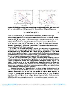
Department of Physics and Institute for Functional Nanomaterials, University of Puerto Rico, P.O. Box 70377, San Juan, PR 00936-8377, USA. 2 Materials Physics and Engineering Division, National Physical Laboratory, CSIR, New Delhi, 110 012, India. 3 Department of Physics, Cavendish Laboratory, University of Cambridge, Cambridge CB3 OHE, UK. ABSTRACT A detailed analysis of leakage current density-gate voltage measurements of gate stacks composed of PLD grown ultra thin films of LaGdO3 (LGO) on p-type silicon substrates with 8.4 Å EOT is presented. Temperature dependent leakage measurements revealed that forward bias current was dominated by Schottky emission over trap assisted tunneling below 1.2 MV/cm and quantum mechanical tunneling above this field. The physical origin of the reverse bias current was found to be a combination of Schottky emission and trap assisted tunneling. Low leakage current densities in the range from 2.3×10⁻³ to 29×10-3 A/cm2 were recorded for films with EOT from 1.8 to 0.8 nm, that are at least four or more orders below the ITRS specifications and its SiO2 competitors. INTRODUCTION Integration of silicon based metal-oxide field effect transistors (MOSFETs) still persists in accordance with Moore’s law [1] by delivering microprocessors with optimized size, performance, and power from one logic generation to another. Active research for alternative high-k gate dielectrics dictated by International Technology Roadmap for Semiconductors (ITRS) [2] commenced in the 1990s for enhanced capacitance density or electrostatic control and reduced gate oxide leakage or stand by power. However it took more than a decade for its entrance into the mainstream complementary metal-oxide semiconductor (CMOS) logic technology. In 2007 the high-k/metal-gate (HKMG) technology was successfully launched in the 45 nm logic technology node to address the drawbacks of high-k/poly-Si structures, such as higher threshold voltages caused by Fermi-level pinning at the interface [3] and severely degraded channel mobility due to the coupling of the low energy surface optical phonon modes (arising from the polarization of the high-k dielectric) to the inversion channel charge carriers [4]. This implementation of HKMG marked a revolutionary change in transistor technology in terms of lower gate leakage, lower switching power, and higher drive current. Later nontraditional scaling methodologies like multi-gate transistors (finFETs) and fully depleted siliconon-insulator (FDSOI) and strained silicon helped in continued scaling down to the 22 nm node.
The ITRS Process Integration, Devices, and Structures 2 (PIDS2) table for future high performance logic technology devices (based on extended planar bulk geometries) demands an equivalent oxide thickness (EOT) of 0.65 nm with a leakage current density of 1.1 × 10³ A/cm2 as early
Data Loading...