Investigation of Recessed Junctionless Double Gate MOSFET for Radio Frequency Applications
- PDF / 1,391,722 Bytes
- 9 Pages / 595.276 x 790.866 pts Page_size
- 108 Downloads / 367 Views
ORIGINAL PAPER
Investigation of Recessed Junctionless Double Gate MOSFET for Radio Frequency Applications Ajay 1 Received: 14 November 2019 / Accepted: 2 January 2020 # Springer Nature B.V. 2020
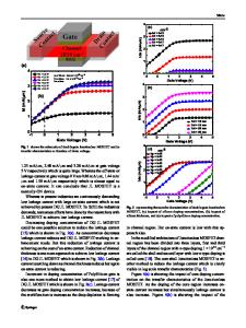
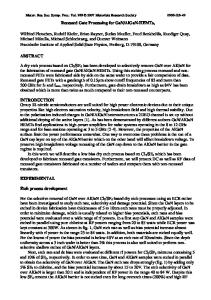
Abstract Junctionless Metal Oxide Semiconductor Field-Effect Transistor (JL MOSFET) is one of the promising candidate to replace the junction based MOSFET for upcoming technology nodes. Semiconductor industries are continuously urging for large ON current with the low OFF current and low specific on resistance. However, high ON current is achieved in Conventional (Conv.) JL DG MOSFET by using high doping concentration at the cost of high OFF current which leads depletion mode operation. Moreover, low doping, narrow channel thickness and high work function gate materials are using to operate Conv. JL DG MOSFET in enhancement mode (Vth > 0 V for N-JL DG MOSFET, Vth < 0 V for P-JL DG MOSFET) but ON current is reduced in all above mentioned solutions. To overcome the above mentioned problems, a new architecture is developed called Recessed JL DG MOSFET. In Recessed JL DG MOSFET silicon region is recessed under the gate region and some gate portion is extended towards source and drain region. Recessed JL DG MOSFET shows the same ON current as achieved in Conv. JL DG MOSFET with very low OFF current (leakage current) by considering high doping concentration. Surface potential, electron density, energy band distribution, drain current have been investigated to proof the enhancement mode operation of Recessed JL DG MOSFET. Figure of Merits (FOMs) for RF performance such as Trans-conductance, capacitance and intrinsic power gain (S21), Trans-conductance frequency product (TFP), Gain frequency product (GFP) and Gain trans-conductance frequency product (GTFP) have also investigated of Recessed JL DG MOSFET. Keywords Double gate (DG) . GFP . GTFP . Junctionless . Radio frequency (RF) . Recessed gate . Trans-conductance . TFP . TCAD
1 Introduction All existing Field-Effect Transistors (FETs) have two junctions at the interface of source/drain and channel. Due to the laws of diffusion and statistical behaviour of the distribution of doping atoms in the semiconductor, the fabrication of ultrasharp and ultra-steep junctions with the high doping concentration at the nanoscale regime has become a great issue for the semiconductor research industry. At the nanometer scale, these junctions lead the Short Channel Effects (SCEs) such as Drain Induced Barrier Lowering (DIBL), punch-through, pinch off, velocity saturation, impact ionization, hot carrier,
* Ajay [email protected] 1
Advanced Nanoelectronic Device & Circuit Characterization Research Group, Department of Electronics System Engineering, Indian Institute of Science, Bangalore 560012, India
etc. which degrade the device performance [1–3]. J. P. Colinge et.al., has presented the concept of Junctionless (JL) MOSFET with fabrication feasibility [4]. Due to absence of junctions, source, channel and drain regions are doped with same type of doping, JL MOSFET seems as n-n-n-type for n-
Data Loading...