A Scanning Tunneling Microscopy Study of MBE-grown GaAs(001)-Faceted Surfaces
- PDF / 2,144,376 Bytes
- 4 Pages / 420.48 x 639 pts Page_size
- 51 Downloads / 330 Views
A SCANNING TUNNELING MICROSCOPY STUDY OF MBE-GROWN GAAS(001)-FACETED SURFACES R. Maboudian,* V. Bressler-Hill,* X.-S. Wang,* K. Pond,** P. M. Petroff,** and W. H. Weinberg*
*Chemical Engineering Department and QUEST, University of California, Santa Barbara, CA 93106, USA **Materials Department and QUEST, University of California, Santa Barbara, CA 93106, USA
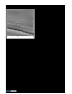
ABSTRACT Scanning tunneling microscopy (STM) and reflection high-energy diffraction (RHEED) have been employed to investigate the morphology of faceted GaAs(001) surfaces grown by molecular beam epitaxy (MBE). The RHEED pattern monitored during the growth indicates that the faceting corresponds to (71 1)A planes. The STM images obtained on these surfaces reveal predominantly a (2x4) local ordering, although unusual (2x3) and (2x6) structures have also been observed. The atom-resolved imaging of the (2x4) structure indicates that the unit cell consists of two As dimers and two missing dimers, identical to the structure obtained on the flat As-rich GaAs(001)-(2x4) surface. Furthermore, islands on the surface are found to be anisotropic, with a shape anisotropy of about 4:1 for step A to step B. The anisotropy is explained in terms of the difference in step edge reactivity.
INTRODUCTION Recently, semiconductor structures having quantum confinement in two and three dimensions have attracted much interest due to their novel physical properties. Several promising methods for the fabrication of quantum-wire structures have been presented, including the growth of tilted superlattices and of grid-inserted heterostructures [1,2]. In addition, periodic faceting of the GaAs surfaces has been proposed as a new approach for obtaining lateral quantization [3-6]. The interfaces of these structures have been studied with transmission electron microscopy, and reflection high-energy electron diffraction has been used to monitor the faceting process during the growth. However, these methods do not provide a detailed picture of the surface morphology on the atomic level. Scanning tunneling microscopy allows in situ analysis of these surfaces, in real space, and directly after growth, and hence, can provide a more detailed understanding of the overall morphology. In this paper, we present RHEED and STM results obtained on a MBE-grown GaAs(001) faceted surface. The RHEED pattern monitored during the growth indicates that the faceting corresponds to (711)A planes. The STM images obtained on these surfaces reveal predominantly a (2x4) local ordering, identical to the unit-cell structure obtained on the flat Asrich GaAs(001)-(2x4) surface. Our results indicate that, under As-rich growth conditions, dimerization is the dominant driving force for reconstruction. In addition, some unusual (2x3) and (2x6) structures have been observed. EXPERIMENTAL SETUP Measurements were performed in an ultra-high vacuum (UHV) chamber with a base pressure of 5x10- 10 Torr. The STM is a commercial microscope described previously [7]. Briefly, the STM head is equipped with Pt/Ir tips that are cleaned in s
Data Loading...