Wafer Thinning for Monolithic 3D Integration
- PDF / 452,805 Bytes
- 6 Pages / 612 x 792 pts (letter) Page_size
- 9 Downloads / 370 Views
E5.7.1
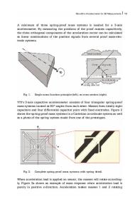
Wafer Thinning for Monolithic 3D Integration A. Jindal, J.-Q. Lu, Y. Kwon, G. Rajagopalan, J.J. McMahon, A.Y. Zeng, H.K. Flesher1, T.S. Cale, and R.J. Gutmann Focus Center-New York, Rensselaer: Interconnections for Gigascale Integration Rensselaer Polytechnic Institute, Troy, New York-12180 1 Aptek Industries, Inc., 414-F Umbarger Road, San Jose, California-95111 ABSTRACT A three-step baseline process for thinning of bonded wafers for applications in threedimensional (3D) integration is presented. The Si substrate of top bonded wafer is uniformly thinned to ~35 µm by backside grinding and polishing, followed by wet-etching using TMAH. No visible changes at the bonding interface and damage-free interconnect structures are observed after the thinning process. Both mechanical and electrical integrity of the bonded pairs are maintained after the three-step baseline thinning process, with electrical tests on wafers with multi-level copper interconnect test structures showing only a slight change after bonding and thinning. This thinning process works well for Si removal to an etch-stop layer, although present process uniformity is not adequate to thin bulk Si substrates. Other issues such as wafer breakage and edge chipping during Si thinning and their possible solutions are also addressed. INTRODUCTION One of the emerging architectures/technologies for future chips is wafer-level threedimensional (3D) integration [1-2]. 3D integration offers high interconnect performance by reducing delays of global interconnects [2] and high functionality with heterogeneous integration of materials, devices, and signals [1-4]. Moreover, monolithic wafer-level 3D integrated circuits (ICs) can accomplish increased functionality over conventional planar ICs, while maintaining the cost advantage of monolithically fabricated interconnects [1-3]. In our approach to 3D integration, Bridge Via Plug Via fully processed wafers are aligned and Dielectric bonded with dielectric glues, followed by 3rd Level Substrate Device top wafer thinning to less than 10 µm (Thinned surface Substrate) using backside grinding, polishing, and wet-etching. Subsequently, inter-wafer Bond Dielectric (Face-to-back) interconnects are formed using a copper 2nd Level Substrate Device damascene patterning process [4-5]. A (Thinned surface Substrate) schematic of the test vehicle for implementing such a 3D integration Bond (Face-to-face) concept is shown in Figure 1. Four key Multi-level on-chip interconnects 1st Level challenges in this approach are; 1) wafer Device surface level alignment accuracy (~1µm), 2) Substrate bonding integrity, 3) wafer thinning and Figure 1. 3D integration concept using waferleveling control, and 4) inter-wafer bonding, with dielectric glue layers, high-aspectconnection. All of these processes need to ratio vias (plug- and bridge-type), and "face-tobe compatible with conventional backface" and "face-to-back" wafer bonding. end-of-the-line (BEOL) processes,
Downloaded from https://www.cambridge.org/core. Columbia University Libraries,
Data Loading...