Die-on-Wafer and Wafer-Level Three-Dimensional (3D) Integration of Heterogeneous IC Technologies for RF-Microwave-Millim
- PDF / 831,359 Bytes
- 6 Pages / 612 x 792 pts (letter) Page_size
- 21 Downloads / 355 Views
G6.8.1
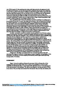
Die-on-Wafer and Wafer-Level Three-Dimensional (3D) Integration of Heterogeneous IC Technologies for RF-Microwave-Millimeter Applications J.-Q. Lu, S. Devarajan, A.Y. Zeng, K. Rose and R.J. Gutmann Center for Integrated Electronics, Rensselaer Polytechnic Institute, Troy, New York-12180, USA, [email protected] ABSTRACT Die-on-wafer and wafer-level three-dimensional (3D) integrations of heterogeneous IC technologies are briefly described, emphasizing a specific 3D hyper-integration platform using dielectric adhesive wafer bonding and Cu damascene inter-wafer interconnects to provide a perspective on wafer-level 3D technology processing. Wafer-level 3D partitioning of high Q passive components, analog-to-digital (A/D) converters, RF transceivers, digital processors, and memory is discussed for high-performance RF-microwave-millimeter applications, especially where high manufacturing quantities are anticipated. Design and simulation results of 3D heterogeneous integration are presented. This 3D technology is applicable to smart wireless terminals, millimeter phased array radars, and smart imagers. INTRODUCTION As the density of RF ICs increases with improved two-dimensional (2D) packaging of chips and vertical three-dimensional (3D) chip stacking, the relative cost of packaging increases as well [1]. While a monolithically integrated system-on-a-chip (SoC) is a worthy long-term objective for digital systems, the heterogeneous IC technologies necessary for high-performance RF systems makes a SoC implementation difficult. While a hybrid assembled system-in-apackage (SiP) implementation is a more realistic objective, the long-term cost of either 2D or 3D die-stack packaging solutions can be affected by chip handling and assembly. Moreover, the performance can be degraded by package parasitics, particularly inductance, as the frequency increases. One viable solution for such RF ICs is a die-on-wafer or wafer-level 3D monolithic integration of heterogeneous silicon ICs. Particularly, with wafer-level 3D integration, digital CMOS, SiGe RF BiCMOS, silicon-on-insulator (SOI) and future silicon technologies can be wafer-level "packaged" with micron-size, through-die, low-inductance vertical interconnects. While the manufacturing technology is not in place for such implementations, various research and development activities are underway. Other key applications driving the technology are three-fold: vertically integrated memory stacks, vertical integration of microprocessors with large L2 cache memory (with reduced access time and cycle time), and smart imagers (such as CMOS imagers with signal processing at each pixel). 3D IC TECHNOLOGY PLATFORMS Three major 3D IC approaches being pursued in various stages of research and development are [2-5]: 1) die-to-die, 2) hybrid die-to-wafer, and 3) monolithic wafer-to-wafer 3D integrations, as shown in Figure 1. Die-to-die 3D integration or SiP is currently used to increase functionality
G6.8.2
Wafers I/Os, A/Ds, A/Ds, sensors I/Os, sensors and glue glue logic and logic Memory Memo
Data Loading...