Channel engineering and junction overlap issues for ultra-shallow junctions formed by SPER in the 45 nm CMOS technology
- PDF / 405,695 Bytes
- 6 Pages / 612 x 792 pts (letter) Page_size
- 2 Downloads / 418 Views
C10.5.1
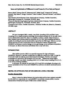
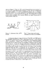
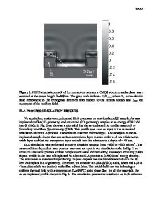
Channel engineering and junction overlap issues for ultra-shallow junctions formed by SPER in the 45 nm CMOS technology node Simone Severia,b, Kirklen Hensona, Richard Lindsaya, Anne Lauwersa, Bartek J. Pawlakc, Radu Surdeanuc and K. De Meyera,b a IMEC, Kapeldreef 75, 3001 Leuven, Belgium b K.U.Leuven, ESAT-INSYS, Kasteelpark Arenberg 10, B-3001 Heverlee, Belgium c Philips Research Leuven ABSTRACT The feasibility of the SPER junction process as a reasonable alternative to the spike anneal junction is proved in this work. Good control of the SCE and performance competitive results as compared to the spike junction are obtained. An analysis of the interaction between the halo dopant and the SPER junctions has been carried out; it is shown that the performance degrades with increasing halo dose as a consequence of an overlap resistance problem. INTRODUCTION The necessity to control the Short Channel Effects (SCE) for the 45 nm technology node and beyond requires the complete suppression of dopant diffusion in order to control the lateral and vertical depth and the abruptness of the junction profile. It is known that junctions formed by Solid Phase Epitaxial Regrowth (SPER) of a doped amorphous region allow for meta-stable high activation levels and perfectly abrupt profiles [1], [2]. In the present work an experimental analysis of the lateral dopant and defect profile obtained by this low thermal budget process is presented through electrical pMOS and nMOS transistors characterization. We observe a strong dependence of the lateral amorphous region near the gate on the implantation parameters used. Unless optimized this leads to poor active doping concentration under the gate that significantly increases the overlap resistance. Through a SPER extension process only, species combinations of Ge, BF2 and B for PMOS, and As for NMOS have been characterized for transistor performance. The issue of HALO deactivation in the End Of Range (EOR) region is studied in detail analyzing the threshold voltage roll-off. It is shown that the degradation in the SCE control can be recovered for both NMOS and PMOS. EXPERIMENTAL In this work NMOS and PMOS transistors processed with a simplified process flow, up to the halo implantation and extension junction formation, have been characterized. The devices are measured probing a large silicon area where deep junctions are present. These probe junctions are implanted after the Shallow Trench Isolation (STI). The different implantation conditions used for NMOS and PMOS devices are described in Table 1. The p+ extension junctions are formed with a Ge pre-amorphization implantation (PAI) followed by a B implantation for incorporating the junction dopant (PMOS1). A BF2 implantation, that allows simultaneously for pre-amorphization and junction dopant implantation is also tried (PMOS2). Similarly the n+
C10.5.2
extension junctions have been formed with a self-amorphized As implant (NMOS). All the processes had previously received a halo implantation with a 1050 oC spike anneal activati
Data Loading...