Shallow Junctions for Sub-100 Nm Cmos Technology
- PDF / 232,534 Bytes
- 6 Pages / 612 x 792 pts (letter) Page_size
- 29 Downloads / 364 Views
SHALLOW JUNCTIONS FOR SUB-100 NM CMOS TECHNOLOGY Veerle Meyssen, 1 Peter Stolk,2 Jeroen van Zijl, 1 Jurgen van Berkum,3 Willem van de Wijgert,3 Richard Lindsay, 4 Charles Dachs,2 Giovanni Mannino,5 and Nick Cowern1,2 1 Philips Research Laboratories, 3 Philips CFT; Eindhoven, THE NETHERLANDS 2 Philips Research Leuven, 4 IMEC; Kapeldreef 75, B-3001 Leuven, BELGIUM 5 CNR-IMETEM, Catania, ITALY
ABSTRACT This paper studies the use of ion implantation and rapid thermal annealing for the fabrication of shallow junctions in sub-100 nm CMOS technology. Spike annealing recipes were optimized on the basis of deltadoping diffusion experiments and shallow junction characteristics. In addition, using GeF2 preamorphization implants in combination with low-energy BF 2 and spike annealing, p-type junctions depths of 30 nm were obtained with sheet resistances as low as 390 Ω/sq. The combined finetuning of implantation and annealing conditions is expected to enable junction scaling into the 70-nm CMOS technology node.
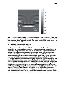
I. INTRODUCTION The semiconductor industry is characterized by an incessant drive for ever smaller and faster electronic devices and circuits. The achievement of shallow, low-resistance junctions is seen as one of the important prerequisites for this evolution. In CMOS technology, the fabrication of shallow source/drain extensions at the edge of the polysilicon gate is the most critical doping step. Figure 1 shows an example of twodimensional doping profiles that were obtained on 0.18 µm transistors, using selective etching and transmission microscopy for the NMOS (Fig. 1a, Ref. 1) and voltage contrast scanning electron microscopy for the PMOS (Fig. 1b, Ref. 2). The contrast fringes in Fig. 1(a) clearly reveal the two As implantation steps by which the junction areas have been fabricated. The drain extension region underneath the spacer is clearly separated from the deeper, highly-doped drain (HDD), as desired. In comparison, the voltage contrast image in Fig. 1(b) indicates that there is no clear distinction between the extension and HDD junctions in the PMOS device. This arises from the fact that boron undergoes much faster diffusion than arsenic due to the phenomenon of transient enhanced diffusion (TED) [3]: ion-generated silicon self-interstitials couple with B atoms during thermal activation, leading to a temporary enhancement in the boron diffusivity. In addition, the excess interstitials drive clustering of B atoms below the solid solubility limit [3], thereby limiting the activation efficiency. These physical effects associated with ion implantation jeopardize the suitability of implanted B junctions for sub-100 nm CMOS. It has been demonstrated [4] that the coupling between silicon self-interstitials and B (and P) decreases with increasing temperature, thereby reducing the driving force for TED. This implies that rapid thermal annealing (RTA), which uses high temperatures and short annealing times, is the most suitable industrial approach for the formation of shallow, electrically active, junctions. The need
Data Loading...