Charging Model of a Si Nanocrystal-based Floating Gate in a Quantum Flash Memory
- PDF / 140,437 Bytes
- 6 Pages / 612 x 792 pts (letter) Page_size
- 97 Downloads / 368 Views
0997-I02-08
Charging Model of a Si Nanocrystal-based Floating Gate in a Quantum Flash Memory Bertrand Leriche, Yann Leroy, and Anne-Sophie Cordan InESS, ENSPS, Bd SÈbastien Brant, BP 10413, ILLKIRCH, F67412, France
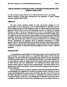
ABSTRACT We propose a theoretical study for charging the floating gate composed of Si nanocrystals (NCs), in a non-volatile flash memory. Only a few electrons tunnel from the channel of a metaloxide-semiconductor transistor into the two-dimensional array of nanocrystals. Our model is based on the geometrical and physical properties of the device, in order to take the dispersion of the relevant parameters into account: NC radii, inter-NC distances, tunnel oxide and gate oxide thicknesses. The energy subbands of the channel are explicitly included, together with the doping density. This three-dimensional model of electron tunneling into a NC is numerically solved through a two-dimensional finite element approach, which allows extensive numerical experimentations. The tunneling times to charge a single NC or the whole NC floating gate are evaluated in a finer detail, and the influence of the dispersion of the relevant parameters is discussed. Such a study may help the experimentalists to build efficient quantum flash memories. INTRODUCTION The quantum flash memories are regarded as a possible extension of the conventional flash memories, in agreement with the last International Technology Roadmap for Semiconductors (ITRS 2005). The first semiconductor nanocrystal memory was elaborated by Tiwari et al. [1], followed then by a great deal of experimental [2-6] and theoretical [7-12] work. This kind of memory is based on a floating gate composed of a two-dimensional (2D) layer of nanocrystals (NCs) in a Metal Oxide Semiconductor (MOS) device. The charges are stored in the NCs, starting from the channel through a thin tunnel oxide (less than 5 nm). Of course, such devices generally present a non-negligible dispersion in their geometrical parameters like the radii of the NCs and inter-NC distances, the tunnel oxide and gate oxide thicknesses. Since we focus on the writing phenomenon of a nanocrystal memory, the device under study is a simplified view for which both the source and drain electrodes are connected to the ground, so a bias voltage is only applied to the gate electrode. A schematic representation of the structure is shown in figure 1a. It consists of a channel, a p-doped Si layer, surmounted of a SiO2 oxide on which a gate electrode is deposited. The floating gate is made of a Si NC layer embedded in the oxide. The Si NCs are supposed to have a cylindrical symmetry but an unspecified crystalline orientation, which is a good approximation for NCs obtained by ion implantation.
Figure 1. (a) Simplified view of the device under study. A Si NC layer is embedded in the oxide of a MOS capacitor with a p-doped Si channel. S and D stand respectively for source and drain electrodes. (b) Geometrical parameters of single NC used to model the whole layer. Figure 1b specifies the geometrical parameters used to mo
Data Loading...