Quantum Analytical Model for Lateral Dual Gate UTBB SOI MOSFET for Analog/RF Performance
- PDF / 2,250,158 Bytes
- 9 Pages / 595.276 x 790.866 pts Page_size
- 50 Downloads / 299 Views
ORIGINAL PAPER
Quantum Analytical Model for Lateral Dual Gate UTBB SOI MOSFET for Analog/RF Performance Arighna Basak 1 & Angsuman Sarkar 2 Received: 30 June 2020 / Accepted: 20 August 2020 # Springer Nature B.V. 2020
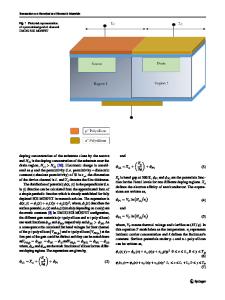
Abstract This paper presents a quantum analytical modeling of UTBB SOIMOSFET as lateral dual gate for the first time. In this paper, a 2dimensional analytical modeling of electric field distribution, threshold voltage (Vth), surface potential and drain current (ID) have been developed and then including Quantum mechanical effects (QMEs)in it. The proposed model provides an expression for Vth shift due to QMEs, which can be used for compact modeling as a quantum correction term. The results of quantum analytical modeling have been verified with the results achieved from numerical TCAD device simulator. Different analog/ radio frequency (RF) performance parameters like transconductance (gm), output resistance (RO), transconductance generation factor (TGF), intrinsic gain (gm*RO), cut-off frequency (fT), gain bandwidth product (GBW), maximum frequency of oscillation (fmax) etc. has been investigated. The effect of negative voltage on the control gate on RF/analog performance parameters has been studied. Result reveals that the potential of UTTB SOI MOSFET with lateral dual gate becomes a choice for analog and mixed signal SOC applications. Keywords Quantum analytical model . Lateral dual gates . Transconductance generation factor . Intrinsic gain . Cut-off frequency . Gain bandwidth product
1 Introduction Over the last few decades, MOSFETs are being continuously scaled down [1]. As a result of this continuous scaling, several deleterious SCEs become prominent and start deteriorating the performances of downscaled device such as Vth roll off, DIBL etc. [2, 3]. To reduce SCEs, researchers have geared towards different technologies like fully depleted SOI MOSFETs [4, 5], Double-gate (DG) MOSFETs [6–8], Surrounding gate MOSFET [9], Junctionless (JL) MOSFETs [10] and Multiple Gate MOSFETs [11]. Moreover, for further reduction of SCEs, UTBB SOI MOSFET [12–15] is demonstrating a high advantage. Therefore, based on this technology a number of alternative approaches such as gate engineering techniques [16, 17], * Arighna Basak [email protected] 1
Department of ECE, Brainware University, Kolkata, West Bengal, India
2
Department of ECE, Kalyani Government Engineering College, Nadia, West Bengal, India
channel engineering techniques [18] and source/drain engineering techniques [19] have been reported for further suppression of SCEs. On the other hand, Wei et al. [20, 21] proposed UTBB SOI MOSFET with the lateral dual gate and triple gate structure for supressing SCEs and justified the impact of negative control gate voltage without showing any analytical modeling. On the other hand, present authors [22], proposed an analytical drain current modeling for this structure for supressing SCEs. In this analytical modeling, QMEs are not incorporated. Therefore, QMEs must be taken into account for scaled dev
Data Loading...