Siloxane Polymers as Low Dielectric Materials for Microelectronics
- PDF / 286,338 Bytes
- 7 Pages / 414.72 x 648 pts Page_size
- 106 Downloads / 380 Views
C. P. WONG AT&T Bell Laboratories, P. O. Box 900, Princeton, NJ 08542-0900
ABSTRACT A modem VLSI device is a complicated three-dimensional structure that consists of multilayer metallization conductor lines which are separated with interlayer-dielectrics as insulation. This VLSI technology drives the IC device into sub-micron feature size that operates at ultra-fast speed (in excess of > 100 MHz). Passivation and interlayer dielectric materials are critical to the device performance due to the conductor signal propagation delay of the high dielectric constant of the material. Low dielectric constant materials are the preferred choice of materials for this reasons. These materials, such as Teflon® and siloxanes (silicones), are desirable because of their low dielectric constant (E 1) = 2.0, 2.7, respectively. This paper describes the use of a low dielectric constant siloxane polymer (silicone) as IC devices passivation layer material, its chemistry, material processes and reliability testing.
INTRODUCTION The electronic packaging trends in the 1990's are toward low-cost and highperformance -2. Non-hermetic plastic packaging is the solution to these requirements. With the advances of IC devices being driven to submicron in feature size, multilayer
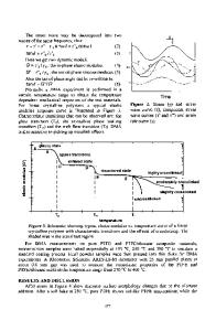
metallization and ultra-fast in speed, low dielectric constant materials are the preferred choice of materials as passivation and interlayer dielectrics. Conventional materials for this type of application are silicon dioxide and silicon nitride. These materials tend to have a higher dielectric constant property that decreases the electrical performance of the IC device. In this paper, we describe a low dielectric constant silicone (eI = 2.7-2.9) as a passivating material of a n-type metal oxide semiconductor (n-mos) IC device. The material chemistry, processes and reliability of the silicone passivated device will be discussed.
EXPERIMENTAL Siloxane Polymers (Silicone) and IC Device Passivation: (A) Material Chemistry: A polydimethyl, phenyl and methyl substituted siloxane with a hydroxyl reactive functional group that is capable to undergo a condensation-cure into a 3-dimensional
89 Mat. Res. Soc. Symp. Proc. Vol. 390 ©1995 Materials Research Society
network is used for this study. An aminosilane, such as (OCH3 )3 Si CH 2 CH 2 NH 2 is also used to accelerate the material cure. (B) Material Processes: (1) Coating of IC Devices: For use as a passivating material, the silicone resin was first spun-on a n-mos IC wafer where a p-glass layer was grown by RF plasma process on these devices. This additional silicone layer as passivating material is used to enhance the device electrical reliability, physically filling any pinholes, microcracks of the R-glass passivating layer. The silicone coating thickness of the wafer was -30,000A. The coated layer was then soft-baked at -150 0 C for 60 sec. to remove the xylene solvent, then further cured at 250'C for 4 hours. (2) Patterning of the Siloxane-Coated n-mos IC Wafer: An adhesion promoter was applied on the siloxane coated wa
Data Loading...